Show by Label

Showing posts with label ESP32. Show all posts

Thursday, February 20, 2025

Creating a Hotplate Reflow Station


This project describes how I converted a UYUE 946C Preheating Station to a reflow hotplate that uses and follows solder paste profiles.


As I normally do on my Blogs, I describe the way I get to the final design, with trials and errors, ups and downs, warts and all, but hopefully in a way that you learn something, and avoid my mistakes. With my projects, it's not going to be an IKEA type quickly-build-it-design. Some effort is required.

Overview

The UYUE 946C hotplate is a 600W 20x20cm device that can be set for a constant temperature by the user interface. There are many variations and versions available with the same model name and for very reasonable prices.

Initially, I wanted to build my own hotplate from scratch, by using a heater and design a controller for it. I even purchased a few different heaters and a thick aluminum plate.

However, after contemplating on how to put it all together, I was not happy or comfortable about the fact that this contraption would be lying on my desk, without a proper enclosure and also dealing with very hot surfaces, and controlling the mains voltage. So for about two years, I stashed the components away, and kept the project on the back-burner. I stayed on the look-out for a solution, but I discounted all oven-designs because they are too bulky for the precious amount of space I have in my man-cave/office. In the mean-time, I investigated a number of DIY controller designs that I liked.

A few months ago, I revisited a YouTube video of a hotplate design I liked earlier, but this time the Maker (Curious Scientist) upgraded it to a new version.

Here is that video: YouTube

I particularly liked the way he shows the reflow curve, and he also shows the actual temperature over time. I was already planning to make my own electronics, so I contacted him for a copy of the Sketch which he gracefully did.

I also ordered the hotplate, but since I knew it would take some time to arrive, I built a prototype for the controller so I could run the software and see what I wanted to change for my version. 


Above is the prototype with the Nano, the original 1.8' 128x160 TFT display, my own rotary encoder with the debounce components and the MAX6675K module to read the K-Type sensor that you also see in the picture.

It took about 2 months for the hotplate to arrive, and in the mean-time I worked off-and-on on the code. At first learning how it worked, but also quickly changing or expanding it to my liking. That turned out to be a much more involving job than I anticipated. All in all, it's a big program with many lines of code (right now there are 2399 lines, but also many with comments)

Changes to the hardware and the code

Here are some of the changes I implemented that were different from the original design. First, I wanted to use an SSR unit, and not deal with my own circuit to control the heater. It would be much easier to keep all the mains related voltages and current far away from my controller.

I also wanted to use a faster processor, because the Arduino Nano that I initially used was too slow to my liking, even though I added hardware SPI to update the TFT much faster. After some time, I also changed the TFT display to a larger version, a 2.8' 240x320 display, based on the ILI9341 controller, and again used the hardware SPI interface to speed things up.

Next I wanted to improve on the rotary encoder code and make it more reliable. Initially, I used my own encoder, but later changed it to the same module that was used in the original version, because I discovered that it has some issues. Some of which was caused by the significantly faster processor, but I also noticed glitches and other issues. First off, the de-bounce capacitors on that module are too large with 100nS, creating a slope that the much faster ESP32 triggers on while in the "dead-zone" between logical levels. Here is what I mean:


The above was taken with a 10K pull-up, another 10K in series and than a 100nF debounce to GND, like it is on the Youmile? or KY-40? module. You can clearly see that there are multiple pulses around the point on the slope where a digital "0" is changing to a "1".


When you zoom in, you can see the real issue in more detail. Realize that every "glitch" is an interrupt to the processor. This is a little less important with slow processors, like the Nano, but a real issue with faster ones, like the ESP32.

So, the remedy is first to reduce the capacitor value to create a more adequate R/C with 10nF, and also use a Schmitt-trigger gate to bring that "slow" ramping signal back to a fast edge again, and feed that single pulse to the processor. It will be a lot happier. 


Note that the above screen is taken with the 10K/10K/100nF values that is standard on these modules. Be aware!


The UYUA 946C Preheating Station

When the hotplate finally arrived, the first thing I did was to open it up before connecting it to the mains. There are numerous situations reported that whatever comes from China does not meet European safety specifications. 


Unfortunately, my unit had the same issue others reported earlier, inadequate grounding of the metal parts to earth. There is no star-washer used anywhere, and at the contact point, the paint had not been removed. Also, the ground lead is a little on the thin side. I will be getting close to 10A, so this needs to be fixed.

That's easy to do though.


Here is a picture of the original controller that I was going to replace anyway.


The other, even more important question I had was what kind of heaters were installed. This was important for me, because I already figured out that 600W was probably not adequate, so I needed a way to add extra heater elements.


This actually looked very good. I was happy to see what I got. There are two round 8mm diameter rods of 350W each inserted in the aluminum profiles. The K-type sensor is bolted in between them, but on the edge. 


First try

After adding another grounding lead from the thick aluminum plate to the bottom, and scraping paint and adding star washers on all connections from the bottom screws to the upper part, and putting it back together.  I could try to see how it worked, and although a bit slow to heat-up, I was pretty pleased.

There was room for improvements.


Adding an additional heater element

The next step was to add another heater element. I already had one, so I cut the flanges off with a hack saw, so it would fit in-between the already installed elements.


The "extra" nuts you see where just about thick enough to use the original screws, but now also pressed the extra heater to the plate.

It worked, but this particular heater element self regulated the maximum temperature to 200 degrees C. When the temperature reached this level, it would stop contributing. 


Adding insulation

To get some more mileage out of the heaters, I purchased insulation sheets with a self-adhesive back, and covered the insides of the top box of the enclosure.


First actual reflow on PCB's

Pretty pleased with this, I tried it out on two new boards I just received for my LORA-based mailbox notifier. It soldered pretty well, although I later found out that the reflow was not long or hot enough for the larger parts, but as a first trial, I was very happy.

At this moment, I was already convinced that this hotplate would only solder low-temperature solder pastes (138 degrees) well enough. Too bad, because I still have a lot of the 165 degree solder paste left, but I could always see what can be done after the units was operational the way I wanted it to be.


Addressing the ramp-up and maximum temperature

In order to address the rather slow heat ramp-up and maximum temperature challenge, I ordered two different kind of elements that would boost the power.


A failed attempt

These round 8mm heater elements are 250W each. I searched and searched for the right profile like the two already installed, but was unsuccessful. Wanting to try it out anyway, I concocted two strips that would hold the three elements in place, and pressed them to the top plate.


It worked, I had a lot more energy available, but when I opened the enclosure again to try the other new element, I got kind of scared.


Worse, one of the aluminum braces was completely burned through.


Wow, this is definitely not the way to go! I may revisit this when I can find the proper profiles to slide these elements into, but so far, I can't find them.


Next trial

Next up, I wanted to try the other heater element that I ordered.

This is a 220V 250 degree C 600W version.

I hoped that it would fit by drilling some extra holes so I could use the original screw holes, but by using longer screws and I mounted it upside down. I did not have the get the hacksaw out, it fitted perfectly.


The fit was just about perfect.


I also changed the K-type sensor to a new one that was more sturdy. To make that fit I had to add a slit into the new element.
I also had to move the tapped hole a little further to the edge. I used an M4 tap. Be careful not to drill too deep.

This is a result by using the "free" Heating mode set to 200 degrees. Most important is the ramp-up period to reach 200 degrees C. (note that the temperature scale is off, the curve is correct, and that has been fixed)


I used my IRmeter to have a look at the resulting temperature on a real PCB using the reflow profile of the Sn42/Bi57.6/Ag.04:


Note that the temperature colors look pretty dramatic, but are less than 7 degrees apart.

I did many, many more tests, mostly to refine the software and tune the ramp-up and overshoot issues, but I also tried out the hardware features. I was still contemplating to use two SSR's to drive the heaters, one for the boost phase, but so far, I have been able to address all of that in the software. 

I also experimented quite a bit with two 12V 80x80mm fans to cool the hotplate down. Now that I know that it all works, I can finish the circuit and start to build a PCB.


The Controller

The final schematic that I'm going to work from looks like this:


It's actually quite simple, but has a few maybe not-so-obvious elements, so let me explain.
I'm going to use a rotary encoder that can be used from the outside of the enclosure. I did not want to use a module, because that is mechanically not very stable. That means that I created the debounce circuits on the main PCB. As I explained above, I'm using Schmitt trigger gates to clean-up the slower R/C slopes of the two critical signals, the ENC-CLK that triggers the interrupt, and ENC-BUT for the pressing of the button. This cannot be used in an interrupt due to the large amount of TFT activity, so this signal is polled. I could have used a Schmitt-trigger chip with two gates, but I don't have that one in stock.

The main power supply is quite simple. I'm using a 220V to 12V-1A power brick and connected that inside the enclosure. The output of that brick goes to the main PCB. The 12V is needed for the fans and is also regulated down to 5V that supplies the components on the main PCB. 

Make sure that you connect the negative lead of the 12VDC also to earth ground of the enclosure. Not only is this safer, it will also remove possible mains related hum from the (extremely sensitive) K-Type sensor.

To the right of the supply is the transistor that I use to control the SSR-40 DA module. The input can be from 3-32VDC, and I'm supplying a PWM signal to regulate the output for the heaters. At first I contemplated using two heater sections and two SSR's, but I could control the heaters tied together in software to mainly avoid overshooting or regulating a constant temperature.

Below it is the circuit to drive the Waveshare 2.4" 240x320 pixel resolution TFT display. This display fits almost exactly in the square hole of the enclosure after I removed the original controller and face plate. The TFT uses the ILI9341 controller. In the software, I'm using the TFT_eSPI library because it's faster then the Adafruit version and allows some extra functionality. When the TFT display is powered-up, it shows a white display all the way up to initializing it. I don't like that, so I added a power on-off circuit that I can control in the code. Normally you would tie the reset signal of the TFT to the reset signal of the processor, but the ESP32 has no pin for that. I can control the reset by a port if needed after the power-up.

To the right of that circuit is the hardware that allows me to control a 12VDC fan, or two fans, like I use in parallel. I will have a DC jack on the enclosure to provide power to the fans.

In the middle is the circuit for the MAX6675 that reads the K-Type temperature sensor. During the prototyping phase, I used one of these modules that are easy to use for that purpose. I'm going to take the chip of that board and solder is on my main PCB.

To the far right is the circuit for the ESP32 with all the connections. The ESP will be socketed on the main board.

The 6 mounting holes below it are for the fastening of the TFT board to the main PCB, and also the main PCB to the enclosure, using the holes that are already there.

Obtaining the correct ESP32 variation

There are many, many variations of the ESP32 board. I'm using a version that is smaller in width and shorter in length. This is my preferred version of the ESP32, because it fits prototype boards. Most of the others are too wide and you have to connect two prototype boards next to each other to make the ESP board fit.

The version I'm using is called the ESP32 DEVKIT V1 from DOIT. There is also one that is virtually the same, called the ESP32 VROOM 4MB DEVKIT V1. If you Google for these names, you will most likely find them. However, there is more to watch out for.

This board only has 30 pins, and the pin rows are about 25mm apart, which is why it will fit in a single prototype board. To make absolutely sure you have the correct version, you also need to look at the available pins on the board. The most important thing to look for are the pins are either end of the board. They must match the picture below.

Even then, there could be two other issues that I describe in a section further below. The board above has the blocking diode installed, visible just below the voltage regulator.


The PCB Layout

The actual layout went pretty fast, although the challenge first was to get the mechanics right with the mounting of the TFT display to it would fit in the enclosure opening, the mounting of the studs to secure it, and the holes to secure the TFT to the PCB.

When I submitted the project to PCBWay for their approval and sponsoring on a Saturday, on Monday I got the go ahead and the funds were in my account. I submitted the final order on Tuesday and I received the boards that same Friday. Even DHL contributed positively this time by passing it through very rapidly without hold-ups at customs. Wow, from order to boards in hand in less than a week, that's impressive!

As usual, the boards have excellent quality. One of the tell-tale signs of quality is the centering of holes in the center of the pad, and they do that very, very well. Always dead center. Another tell tale sign is the crispness of the silkscreen, even with smaller fonts. One more tell tale sign is the plating of the (mounting) holes in the board. The insides are well plated and also connected to the outer ring. The hole positions and sizes are perfect.

In any case, I stuffed the PCB and reflow soldered it on the hotplate with the prototype controller. It went very well, there was only one suspicious soldering joint (too cold) and one solder blob between the pins of the tiniest part on the board. That was easily fixed. I was using the 14-bit MAX31855 instead of the MAX6675, but I found that the reported temperature is a little jittery, causing the reflow curve to be a lot less smooth. Just a bit of warning if you consider using this part. We don't need more than 12-bits, and the MX6675 is actually cheaper.


Bummer!
When I added the THT parts after the reflow soldering, I noticed a goof with the rather special mounting block for the K-Type sensor. I took that from the circuit board module that I had been using so far, together with the MAX6675 chip. I used the standard 5mm spacing for the layout, but this connector is larger. For the time being, I'm using a 5mm version, but I corrected the layout.

The rest of the mounting was pretty uneventful, although I did not mount the TFT screen yet. It will have to be soldered onto the board connector pins at the very last minute, because removing it later on is going to be a pain. There is no room for a socket or header.

After an inspection and a flux clean-up, I tested the various circuits by just using a DMM and my power supply, and verified the rails. I also tested the activation of the voltage regulator for the TFT, and that seems to work as well, but that was without the TFT connected.

Another bummer: a KiCad issue - watch out!

I added headers for the ESP32 DEVKIT1, but when I wanted to mount the board, it did not fit. I used the standard ESP32-C3-DevKitM-1 footprint, in the understanding it was the correct one. You should know that most ESP32 boards are wider than most others, like ESP8266 or Arduino Nano's. It's a real gotcha.
Well, it got me. I used the ESP32DEVKIT1 in another project without issues, so at first I didn't get it. 

After some searching, I found the root cause. I recently upgraded KiCad to version 9, and I now noticed that my own footprints and symbols were not migrated and installed, although I said yes when asked for the migration for the previous version of KiCad during the installation.

Looking at the documentation in more detail (RTFM!), I now noticed that user libraries are not installed, you have to do that by hand. In my own footprint library, I have the correct version for the ESP32DEVKIT1, so the fix was easy, but I'm now left with a board that needs some surgery.

In any case, this is how it looks like:


The board is actually shown upside down, but you can see that the TFT is mounted on front of the PCB, together with the rotary decoder, facing the outside of the enclosure. The 8mm M4 mounting studs allow me to secure the board inside the window of the enclosure that becomes free when you remove the older stuff. The enclosure already has holes for the mounting, although I needed to drill them out to 3.5mm and counter-sinked (sunk?) them on the front.


This is the back of the PCB, facing the inside of the enclosure, where most of the parts are located. Top left is the replacement connector for the K-Type sensor. The TFT display is mounted using the studs and screws that it came with. I just added two screws to mount it on the PCB.

Please take note that the -12V input, or the wall-wart GND, also gets connected to the earth ground of the enclosure, which is securely connected to the earth ground of the 230V receptacle. 

To the right are the headers for the ESP32, that are now too close together. A major goof. 


I have ordered some more ESP32DEVKIT1 modules without the connector pins soldered, and I'm hoping I can bend the pins and the headers such that it will fit, otherwise I have to figure something else out, or order new boards. I already fixed the layout so we now have Version 2.1 although there are no schematic changes as yet. I hope I can brute force the ESP into the headers so I can give it all a try to make sure it works before I order new boards.

I tried a few things, but the board continued to pop out of the sockets. I finally created a set of extenders that allowed me to plug-in the ESP32 board and verify the rest of the controller. And then, I found another foot print error, this one for the 2N3904 transistor. There are SMD foot prints that swap the B and E connections, and yet, I picked the wrong one. I tested it by flipping the transistor upside down which would flip back the E and B leads. Then there was a filter capacitor that I placed not where it should be (close to a chip). 

I fixed the four layout errors and ordered new boards that PCBWay gracefully sponsored again, despite my goofs. They arrived quickly so I could build-up a new board to give it another try. This time it seemed to work, but as soon as I turned the heater on, the screen went blank, the controller powered down and went through a reset. Oh bummer, now what? 

I had been using this setup for several weeks now, and thoroughly tested it, I thought. After some tests, I found out that it was the 12VDC wall-wart that caused the problem. It is a very, very old 1Amp supply that I hadn't used in years, but it worked for several weeks without an issue. My take on it is that one or more capacitors inside the supply probably gave up on me, and just adding 50mA or so when the SSR was activated caused the supply to drop the voltage. Replacing it with a more modern and beefier unit fixed it all.

Here is how it looks now with everything installed and working.


I have not figured out yet what I'm going to do about the left and right side of the TFT. It's functional, but does not look that nice. Unfortunately, I don't have a 3-D printer (yet?) so it will have to be like that for a while, or I can figure out to create a small window-frame from mylar or something like that..

Here are pictures of the inside:


The black box in the background is the 12VDC wall-wart that powers the controller and the fans.
To the left is the SSR.

In the top right corner is the 12VDC chassis part that the fans plug in to. Make sure that this DC chassis part is isolated from the metal frame because the minus connection for the fan(s) is not earth-ground! If the minus of the Fans is at GND/EARTH level, the switching MOSFET is bridged/shorted and the fans will run at full speed and cannot be turned off by the controller. Feel free to use another connector for the fans, I used what I had in stock, with this caveat.


K-Type Thermocouple color coding

It is important to connect the proper K-Type thermocouple leads to the connector and hence the MAX6675 inputs. There is a positive and a negative input. The color coding for these thermocouples is rather strange, but this table explains it all. According to this table, I have the German DIN13711 color coding because the wires from my K-Type are Green and Red. So according to this table, Red is positive and Green is negative.


The MAX6675 blew itself(?) up

When I was using the reflow oven, it suddenly developed an issue with the temperature reading. It turned out that the MAX6675 developed an internal short between a thermocouple lead and VCC. When I investigated this, I saw that the MAX6675 reported a status error 4, indication just that, a short. The result was that the temperature reading was 1024 degrees, obviously this is the maximum possible reading with a 12-bit ADC.

Replacing the chip solved the issue, but I also found out that I probably made a mistake that could have contributed to the demise of the chip. According to the datasheet, you should connect the minus lead of the thermocouple to circuit GND. I did not do that, under the impression that the floating input with the braided and grounded cover would take care of that. Apparently not, so I stand corrected. The fix is easy, just connect the minus lead of the thermocouple to circuit GND by soldering a short wire from the connector pin to the ground plane.


ESP32 Board Caveat

When I was researching the defective MAX6675 issue, I also stumbled into another trap that I already knew but overlooked, the ESP32 board caveat. There is a potential problem with some of the ESP32 boards that may bite you. If you are familiar with these Arduino and ESP boards, you will know that there is normally a blocking diode on the board that prevents back-feeding the 5V through the USB connector to your PC. However, on some of the ESP32 boards, this diode is missing, and the manufacturer installed a 0 Ohm resistor instead.

This is not an issue when you feed the 5V from the USB port to the ESP32 board, but if you power the ESP32 board from a voltage from your board, you will send a current of several hundred mA to your PC. Not only is this an unhealthy situation for your PC, but also the voltage regulator on your board may not be able to sink that much extra current.

During the design phase, I used an ESP32 board that had the diode in place, there is a picture of it further up, so there was no issue. However, I decided to use another ESP32 board in the final version with the corrected PCB layout, which was OK, because I didn't need a USB connection when operating the reflow controller.


The picture above shows the rather interesting way of soldering the reset capacitor to the EN button on the left. What is more to the point, in the middle is the blue arrow pointing to the 0 Ohm resistor that should have been a 5V blocking diode.

So, when I found out that the MAX6675 was showing problems, I was debugging this with the USB port connected, so I could use serial monitor to see what was going on. That was working fine, until I burned my finger on the 5V regulator. I quickly realized what the problem was, and remembered the root cause that I already found when designing the Dynamic DC load that has the same issue.

There are a few remedies:
  • Do not use the USB connection when you power the ESP from the controller board.
  • Remove the 0402 0 Ohm resistor from the ESP32 board. However, that will prevent you from powering the ESP32 solely from the USB port. You could add a 0402 Schottky diode in place of the 0402 resistor, but that's tricky if you use a heat gun.
  • Install the blocking diode on the controller board by cutting the 5V supply trace and install the diode there. (Cathode towards the ESP32)

Redesign of the PCB to V2.2

Because of the two above mentioned issues, I made a few corrections to the schematic and redid the layout to accommodate the grounding of the thermocouple lead, and I also added improved grounding for the MAX6675 as well.

Second, I also added the possibility to either install a 0 Ohm resistor in the 5V path to the ESP32 if your ESP32 board already has the blocking diode, or install the blocking diode on the controller board if your ESP32 board does not have it.

The Github site and the PCBWay Shared Project now have the V2.2 layout.


In the meantime, I did solder a rather large (123x83mm) and pretty complex PCB with many parts. large and small for new project, and that worked well. So with the latest changes to the controller, I'm happy to have this additional tool. It's a huge time saver compared to a heat gun, and it's also much easier for soldering larger components like large size Tantalum capacitors.

Using fans

I looked at integrating the fans into the enclosure, but things get too hot, and the effectiveness would not be great anyway.

If your going to use the optional fans, have a look at the pictures below to see what I concocted instead during the prototyping phase. This actually worked so well that I kept it that way.  The fans are 12V 80x80mm, and I used an aluminum strip to mount them side by side. I then used one of those cheap flexible circuit board holders to position them such that they blow across the surface. The 12V power wires are soldered to a 12V plug in parallel.


Warnings!

The code that I wrote only works with Visual Studio Code (VSC), and NOT with the Arduino IDE. The reason for this discrepancy is the difference in libraries for the display and the way you need to address the SPI bus ports. There have been a few makers that built the hotplate, but ran into issues with the display. It stayed blank. They used the Arduino IDE.

It has been pointed out that I connect the MAX K-type convertor to 5V, while the ESP32 is a 3V3 device. This is no problem for the CS and SCK signals because they are generated by the ESP and the MAX can easily handle these voltages. The SO signal is an output from the MAX and goes to a 3V3 level input of the ESP.  The internal (ESD) protection diodes for the ports will normally take care of this.

According to the above datasheet, the SO output has a drive capability of only 1.6mA. This is low enough for a short burst for the ESP32 inputs, and should pose no problem.

If you are concerned about this, there are three remedies that you can apply to the current PCB. You can cut the SO trace and add a 1K series resistor lowering the current some more. You can add a (Schottky) diode with the Anode connected to the SO pin of the ESP32, and the Cathode to the 3V3 output pin 16. This will clamp the SO voltage to the 3V3 level, and will help the internal clamping diode of the port, that has a lower capacity.
The last remedy is to cut the 5V VCC trace to the MAX chip and use a small patch wire to connect it to the plus of C12, the 3V3 supply. I have not verified any of these changes.

When I decide to do a new board turn, I will consider making the VCC change, but need to verify the proper operation before I will publish this change.


Github repository

I have created a Github repository with all the design information. It can be found here.

There is also a shared project on the PCBWay site so if you want to order PCB's, populated or not, you can go there


I may be adding information for a while while I'm collecting data from reflow soldering actual boards, so stay tuned! Keep in mind that you may have to tune the software to adopt the reflow profile to the actual results. Your heating elements -will- be different from those that I'm using.


Friday, September 20, 2024

Building a DIY Dynamic DC Load

 VB Dynamic DC Load

Construction and Build Instructions
Calibration & Verification
Battery Tester


[UPDATE] March 17, 2026

Bud and I teamed up again to enhance the firmware, and design a completely new ported version for the Batt Tester application. The two are now very tightly integrated, and have many new enhancements and more automatic settings making it even easier to use. As a small example, when you start the Batt Tester app and connect a serial port to the Dynamic Load, it will automatically enter the BT Mode, and is ready to accept the parameters to start a discharge test.

The Batt Test app has been ported from Delphi-7 to Python, making it also portable for Windows, MacOS and Linux platforms.

The DL firmware has seen some significant improvements, making it more reliable and more precise. I switched from the Arduino IDE to Virtual Studio Code and platform.io, taking advantage of the much more advanced programming environment. Especially the BT mode, but also the CV mode has been upgraded. Instead of recompiling the code with a different calibration value, we have added a native calibration mode that accepts commands to enter the values over a serial connection. All you have to do is to keep the rotary encoder button pressed during the boot sequence.

We have provided binaries for the DL that can be uploaded without building the code yourself, and an executable .exe file for the Windows Batt Test app. MacOS and Linux executables need to be build on those platforms, and we provided detailed instructions for you to do that.

The original Github repo has been completely reorganized and is updated with all the hardware and software sources, executables, build instructions and very detailed readme files.

NOTE
During the testing of the new Calibration Mode, we stumbled into a nasty artifact of serial monitors resetting or even hanging the ESP (or Arduino boards). This is not new or a firmware issue but is a result of how serial monitors implement the RTS/DTR activity in combination with the two transistor circuit on all ESP and Arduino boards. We have a hardware fix for the starting of these monitors by populating C44 on the DL PCB with a 22uF value capacitor. Closing the monitor will need a workaround that we provide and describe in the documentation below. Previous builders of the DL should now always add C44.

Here is the Github repo for the project: https://github.com/paulvee/Dynamic-DC-Load


Build instructions for the hardware

Below is a list of items and instructions that will help you to build a Dynamic DC load instrument. 

The design process for the instrument is documented on this Blog here:
https://www.paulvdiyblogs.net/2024/04/build-diy-dc-dynamic-load-instrument.html

The two BOM's, Gerbers, Firmware and other required files can be downloaded from the GitHub. Note that I recently added files that Bud created and will allow you to 3D print your own enclosure and that includes the backpanel and feet.|
https://github.com/paulvee/Dynamic-DC-Load

I also added the instrument details as a Shared Project on the PCBWay site so you can order the boards directly from there:
https://www.pcbway.com/project/shareproject/DIY_Dynamic_DC_Load_8643ddca.html
https://www.pcbway.com/project/shareproject/DIY_Dynamic_DC_Load_Face_PLate_12899b9c.html
https://www.pcbway.com/project/shareproject/DiY_Dynamic_DC_Load_Back_PLate_cda4ffcf.html

Bud, the designer of the instruments hardware core, started his own Hackaday project to document the design here: https://hackaday.io/project/195380-dynamic-electronic-load
I took all his stuff from there and copied it in the design process Blog, so it's all in one place.


The Specifications:

  • Input voltage: 1..100VDC.
  • Reverse polarity protection to -100V and a 10A fuse.
  • DUT is disconnected by a relays for invalid inputs like reverse polarity.
  • Maximum current of 10A @ 40V
  • Maximum power 180W @25 degrees ambient temperature (heatsink temp 85C)
  • Off state DUT current 1.9uA at 2V, 57.7uA at 60V.
  • Volt Accuracy: 0.4%
  • Current Accuracy: 0.4% (using a two-point calibration for best precision)
  • Native Calibration mode with commands entered over a serial connection
  • Power input: 12VDC Wall-wart 0.5A with reverse polarity protection to -24V and PTC fuse
  • CC, BT & CV modes with real-time operation regulated with hardware.
  • In the BT mode, the operation is controlled by a seperate App that is tightly integrated.
  • CP and CR modes have active regulation supported in software (resolution +/-156uA).
  • Pulse/transient mode supported by an external Function Generator. 5V=10A
  • Current monitoring with a DSO. 1V=10A
  • GUI: 128x128 OLED 1.5' color display and a rotary encoder with dual button functions.
  • Two temperature controlled fans.
  • Protection for over voltage, over current, over power and over temperature limits
  • Watchdog protection for stalled software and for the serial connection in the BT mode
  • Overall dimensions: 21cm long, 18cm wide and a height of 118cm.
  • Weight: approx. 1110 grams

  • Parts & Components

    I will show a few parts and components in this description, but all the main PCB parts are listed in a BOM with their order numbers, and the additional off-board parts are listed in a separate BOM, both are available on the Github site.


    The Printed Circuit Boards

    The Printed Circuit Boards (PCB's) are available through PCBWay, who are sponsoring my activities by providing the PCB's free of charge. I have been using their service for several years now and the boards are of excellent quality, every time.


    To create a professionally looking instrument, and to aid with the construction, I have also created a front panel and a back panel PCB. Both also available through PCBWay.


    The back of the front panel has 4 solder pads that can be used to glue the OLED display into position, so the visible portion will be positioned in the middle of the square cut-out.

    NOTE Bud designed an enclosure that can be 3-printed, and that includes a backpanel. See the Github for the .stl files.


    Stuffing the PCB

    Adding components to the PCB should be a straightforward job, except maybe for soldering the minute packages for the ADC, the reference, the two analogue switches and the MCP6V51 Opamps.

    I highly recommend you use a socket for the ESP32. To that extend, make sure you order the WROOM 4MB DEVKIT V1 module without the headers installed. The one below has the blocking diode installed, more details below. Note the pin layout and make sure you get one that has the same layout!

     I use the following headers and sockets for the ESP32, I buy them by the strip.


    To add the components to the PCB, my recommendation is to start with all the passive components like resistors, capacitors and then the active transistors, MOSFET’s (not the main NFET’s M1, M2), diodes and the voltage regulators U9 and U12. Do not install the relay and the snubber circuit yet. What I then would do is to connect a Lab Power Supply with a setting of 12V and 50mA to the DC input of the board. If it powers-up without getting into current limitation, you will probably not have any shorted rails to ground, and can proceed to test the +12, +9 and +5 supply voltages. If they check-out, you can add the ICL7660 and test the -5V rail. After that, you can add the REF5040 and check the presence of  4.096V. If that also checks-out, you can add the trimmers, connector strips, DAC, ADC, MOSFET switches (U14, U15), all the Opamps and finally, the main relay and snubber circuit. Basically, everything except placing the ESP32 module in its socket, and soldering the main NFET’s (M1, M2) and the LM35.


    Obtaining the correct ESP32 variation

    There are many, many variations of the ESP32 board. I'm using a version that is smaller in width and shorter in length. This is my preferred version of the ESP32, because it fits prototype boards. Most of the others are too wide and you have to connect two prototype boards next to each other to make the ESP board fit.

    The version I'm using is also called the ESP32 DEVKIT V1 from DOIT. If you Google this, you will most likely find them. However, there is more to watch out for.

    This board only has 30 pins, and the pin rows are about 25mm apart, which is why it will fit in a single prototype board. To make absolutely sure you have the correct version, you also need to look at the available pins on the board. The most important thing to look for are the pins at either end of the board. They must match the picture below.

    Even then, there could be two other issues that I describe in a section further below. The board above has the blocking diode installed, visible just to the left in the pic of the voltage regulator.

    The other recommended ESP32 board is the VROOM 4MB DEVKIT V1. 

    However, I have found that there are slight variations or differences for two components on various sources for this board. One is the capacitor that should ensure a reset after a download of new firmware. On one of my boards, this capacitor was there, but not well soldered to the chassis part of the USB-mini. On another one, there was no diode to block the incoming 5V through the USB, and the VIN supplied to pin 1 of the board. Having no diode but a 0R resistor means that the VIN supply will back-feed 5V into the USB port of your PC. Not recommended!

    To avoid having to mess with the ESP board and 0402 size parts, we have made provisions on the DL PCB to help fix these two issues.

    Verify that the ESP32 module has a 1uF 0402 capacitor most likely connected to the solder pad of the EN button. It may be soldered at a 45-degree angle, see the left blue arrow. If the capacitor is not installed, you need to install C44 on the PCB. (in the schematic C44 has a red cross through the part, to avoid placing this part when not needed) 

    UPDATE: To circumvent serial monitors used in the new calibration procedure rebooting the ESP32, you now have to always install C44 with a ceramic 22uF 0805 value!

    Also make sure that there is a diode installed and not a 0 Ohm 0402 resistor (marked 000) as you see here on the board. See the middle blue arrow below for the location. The picture of the ESP32 further up in the Blog does have a diode, which can be easily identified.

    If there is a 0 Ohm resistor on the board, you need to either remove it or do not install R53 but install D10 on the main PCB. See the schematic below. (in the schematic D10 has a red cross through the part, to avoid placing this part when not needed)


    The Back Panel

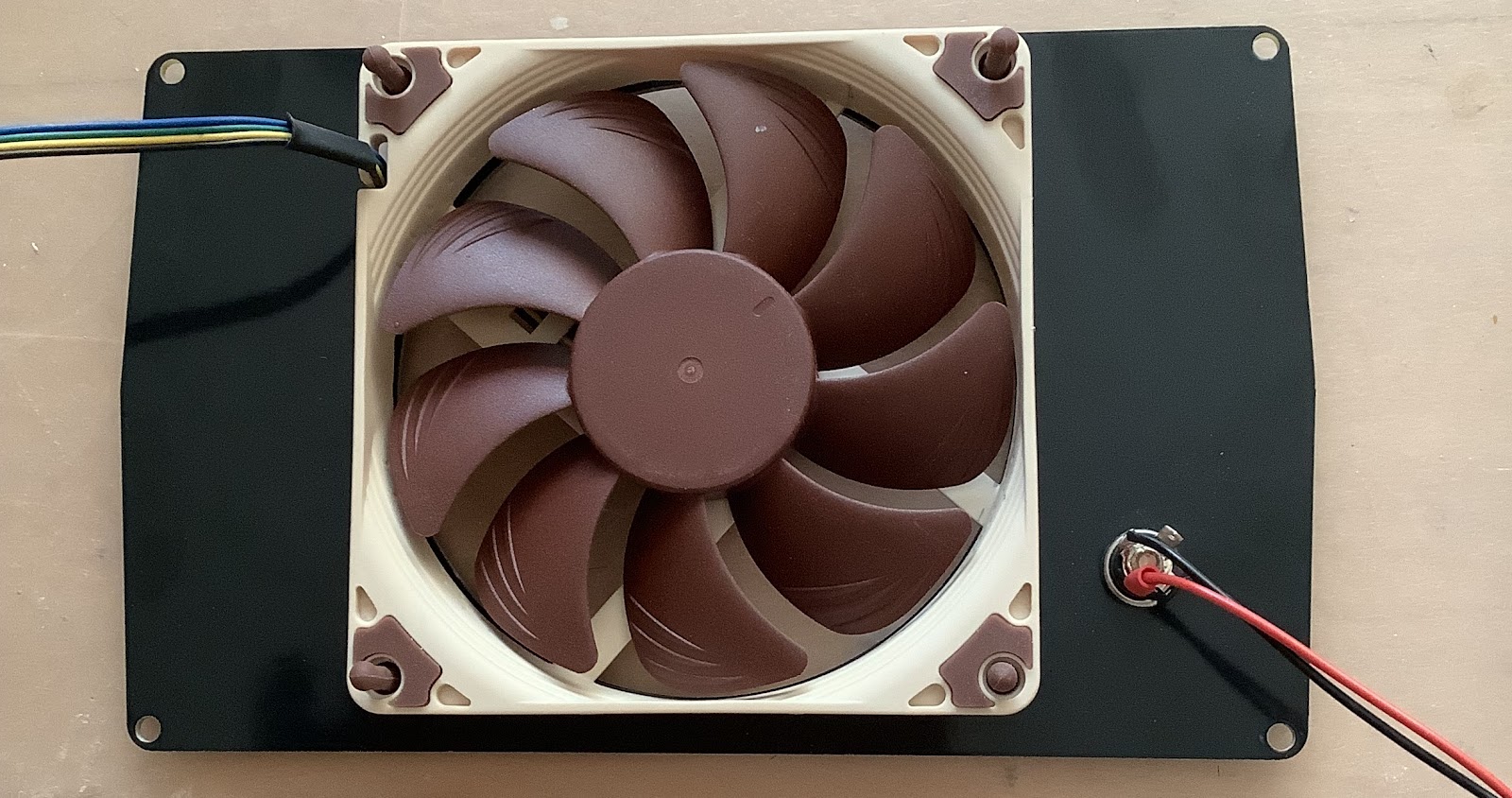
    At this moment in the build process, it will help to mount the fan on the back panel so you can use it to double check the space between that fan and the second heatsink/fan combination that will be mounted on the bottom shell later.

    The back panel fan will be mounted using the flexible silicon mounts that come with the fan.

    To help the installation by pulling on these flexible thingies, it is helpful to first counter sink the 4 holes in the PCB on either side so the silicon will more easily slide into position when you pull them in.


    Note the position of the fan on the back panel, and where the wires need to come out (top left).

    The four wires from the fan come standard with a pretty stiff heat-shrink tube. That's too stiff to my liking, so I cut it off, exposing the four wires.


    Modifying the enclosure

    The bottom shell of TEKO AUS33.5 enclosure needs to be modified so we can mount a fan on the bottom to suck fresh air directly into the heatsink fins inside the enclosure. The fan mounted on the back panel will suck the hot air away from the heatsink to the outside of the enclosure.

    A number of holes need to be drilled in the bottom shell to get enough airflow to the heatsink. I used Excel to create a raster for the 6mm holes. The picture shows an earlier position of the fan, I later moved it further down and added another number of extra holes.


    To feed plenty of fresh air from the bottom of the enclosure to the fan, we need to mount 4 feet that are about 1cm in height to lift the instrument from the shelf or desk to create the space.


    The bottom fan needs to be mounted in the middle of the enclosure, and the mounting holes 25mm away from the back edge of the bottom shell, to make room for the fan that is mounted on the back panel. Before you drill the holes, use the back panel with the fan mounted on it to double check the space you need. The minimum space between the two fans should be at least 2mm.


    The bottom fan and heatsink

    The bottom fan will be mounted on the shell by four 30mm long M3 screws. Because of the plastic, and the two hole positions in the ventilation area, I recommend you put M3 or M4 rings on the bottom and on the inside of the plastic shell. Use a normal (flat) M3 nut to tighten the four screws to the enclosure while making sure that the fan will easily fit. After the fan is positioned on the four mounting screws, use an isolated M4 ring (teflon?) on top of the fan before you mount the brackets holding the heatsink.

    The heatsink will be mounted about 6mm above the bottom fan by two strips of a 90 degree angle 15x15mm piece of aluminum. These strips can be found in your local hardware store and probably come in a length of 1mtr. Use a metal hacksaw to cut two pieces with a length of 90mm, which is the same as the size of the fan. Drill two holes of 3mm each 15mm from each end, that will hold the self-tapping screws mounting the bracket to the heatsink.

    I used very short 3mm self-tapping screws to mount the angle pieces to the heatsink. I also drilled the hole through the second flange of the heatsink, to make room for the tip of the screw, so it does not bend the thin flanges.

    Drill two more holes in the other flank of the L-shape brackets that are 81 mm apart, so the screws holding the fan to the bottom of the enclosure will go through these holes. Make sure that these holes are spaced such that when the L-strips are mounted on the heatsink, the holes of the fan will pass through the four 30mm long M3 screws.

    Because the heatsink can get very hot, I used four 3mm insulating rings of the type that are used to mount TO220 type devices isolated to a heat sink. For us they also serve to electrically isolate the screws from the potential of the heatsink, that can be up to 100V DC. The two NFET's are not isolated from the heat sink to get maximum heat transfer, that is the reason the heatsink will be at the voltage potential of the DUT voltage.


    You’ll need a fifth one to isolate the LM35 from the heatsink later. These rings should fit the holes of the brackets, if not, drill the holes a bit larger to 3.5-4.0mm to create some wriggle room. I then used a Teflon ring on top of the insulators and used self-locking M3 nuts to loosely secure the heatsink, so you don’t need to tighten the nuts too much and put too much pressure on the plastic frame of the fan. You want to minimize the transfer of the mechanical vibration from the fan to the enclosure. It should be a fairly loose fit. 

    The thermal paste you see in the pictures is because I took my instrument apart to make these instructions and the pictures after I finished my build.


    Mounting the Main NFET’s and the LM35

    Before you mount the heatsink on top of the fan, you need to create three M3 tapped holes in the heatsink to mount the two NFET’s and the LM35 temperature sensor. If you don’t have a good quality and sharp M3 tapping set and the right size drill (2.5mm), you can also use 3mm self-tapping screws. In that case it is even more important that you counter-sink these holes well after drilling, so the aluminum material does not come-up and push the devices up from the heatsink when you fasten the screws. If you use the M3 taps, lubricate the drill and the taps well and clean the taps and lubricate them regularly while you are tapping, to make sure that the threads are not damaged. The NFET’s and the LM35 will need to be tightened to the heatsink well, to get the maximum heat transfer, so the threats need to be well made.

    I created M3 threaded holes for the two NFET’s 23mm from the back-end of the heatsink, 33.5mm apart, and each about 23mm from the edge of the heatsink.

    The LM35 goes in the middle of the heatsink and 27mm down from the back. Countersink the holes and make sure everything is flat. Use a fine file or very fine sandpaper with a stiff support if needed.


    The other four holes you see are from previous mounting positions and are no longer used.


    The front of the main PCB will be supported by two extenders towards the front of the enclosure. I used two 30mm long M3 extenders screwed together. You can use any length parts, as long as they are 60mm in total. The height can be further adjusted when the PCB is mounted. The position of the holes in the bottom enclosure for these supports is best determined when the PCB with the NFET’s and the LM35 is mounted on the heatsink.

    As you can see from the picture below, the bottom fan is positioned such that the wires come out at the left-hand side. The open side of the fan must be facing the bottom of the enclosure so it sucks the air into the enclosure. 

    Because the four wires for the fans have a shrink-wrap tube, they are too stiff to my liking, so I took the tubing off.


    The NFET’s and the LM35 will be mounted flat on the heatsink. The main PCB needs to be mounted as high as possible away from the heatsink, to minimize heat transfer. With earlier prototypes, I found that there is a surprising amount of heat transferred through the NFET leads to the PCB. Keeping the legs long helps.

    The challenge is to move the body of the NFET's as far away from the PCB as possible, to again reduce the heat transfer by way of the leads, and also the heatsink heating the bottom of the PCB. We also need to create space away from the PCB to mount the two smaller TO220 heat sinks on top of the NFET's without them touching the PCB. The place where you bend the leads of the NFET's upwards is critical to accomplish this. I bend the leads of the NFET's after about 6mm from the case with 90 degrees (not too sharp!) upwards. 


    You can position the three devices loosely with a screw using the M3 holes you created earlier, and then position the PCB on top of them, with the leads protruding through the holes in the PCB. At this moment, you can use the two mounting extenders to support the other end of the PCB so it is about horizontal, or use something else to keep the PCB horizontal and stable. I also used two spacers of 8mm to support the PCB near the NFET’s so you can position the PCB horizontally in order to solder the leads, and keep them the right amount away from the PCB. Make sure that the PCB is positioned high enough such that the NFET leads only just protrude 1-2mm through the PCB holes to allow for proper soldering. The LM35 leads are a bit longer, so that’s OK. I suggest that at first you solder only the middle leads at this moment. Be careful not to drop the other end of the PCB and bend the NFET leads.

    Once you are happy and double checked the position of the PCB and the three devices, you can mark the position of the two front supports in position on the bottom shelf and then remove the three screws holding the three devices and remove the two extra 8mm standoffs.

    You can now finish the mounting of the two front supports by drilling the holes in the bottom enclosure. I suggest that you use 3.5 or 4mm rings on both sides of the plastic for support. After you have secured the bottom portions of the extender to the enclosure, you can roughly adjust their total height by the second extender. 

    Before you finally mount everything again, apply heat paste to the NFET positions on the heatsink and use an insulated silicon pad with an insulator ring for the LM35. Loosely tighten the 3 screws again and use an Ohmmeter to make sure that the LM35 tab is insulated from the heatsink, because the NFET’s are not, and their pads will connect to the DUT voltage of up to more than 100V to the heatsink.

    When everything is in position, you can tighten the screw for the LM35 and again check that the tab is still isolated. Unscrew the two NFET’s screws again and now add the extra TO220 heatsinks on top of them, using plenty of heat transfer paste.


    Make sure that the heatsinks do not touch the PCB. You can now carefully tighten the screws for the NFET’s.

    After that, you can do a final adjustment of the two front supports so that the PCB is horizontally mounted inside the enclosure. When that is done, re-heat the middle pins of the three devices, to let the stress out, and then solder the other pins. Use plenty of solder for the NFET leads, they will get stressed by the developing heat (up to 100 degrees C).


    Preparing for a first power-on

    After you have finished the above steps, we can start to power-up the board again and verify some of the vital signs.

    You only need to add the 12V DC power to the board, but I recommend you use a Lab supply initially with a current setting of 100mA. If there is no large current, indicating a short or another issue, you can now switch to the 12V DC wall wart.

    Do not install the ESP32 in its socket at this moment until you have verified the power rails.


    Verifying the Power Rails

    You can now verify all the power rail voltages:

    ·         DC Input 12...15V at J4

    ·         +12...15V at pin 1 U9 (LM7809)

    ·         +9V at pin at pin 3 of U9

    ·         +5V at pin 3 of U12 (LM7805)

    ·         -5V at left side of C31 or pin 5 of U5 (ICL7660)

    ·         +4.096V on either side of R60

    When that is OK and within specifications, you can go to the next step, but first disconnect the 12V DC input again.


    Adjusting the OLED display in position on the front panel

    The OLED module connects to J6 on the PCB. The display module comes with flying leads that each have their own 1-pin connector. I recommend you change these single connectors to a 7-pin connector so you can’t make mistakes with the order, and it’s a lot tidier and easier to remove and install.

    Do not apply the main 12V at this moment, it is not needed for this step.

    For this step we need to install the ESP32 module on the PCB and load the ESP32_OLED_Test_V1.ino firmware. This file is located on the Github site in a folder with the same name.
    Here: https://github.com/paulvee/Dynamic-DC-Load

    Locate the file and download it to your PC. Save it in a new directory called “VB Dynamic DC Load” in a directory on your PC. It will only be used once.

    After you saved it, you can use the Arduino IDE, or VSC to locate the file and load it into the IDE.

    You can connect your PC to either the mini-USB of the ESP32 module, or start to use the mini-USB to USB-C adapter. When you have made the connection, the red power LED on the ESP32 module should light-up and your PC probably will give a signal that a new device is connected.

    After loading the firmware in the Arduino IDE, in Tools select Board and search for the DOIT ESP32 DEVKIT V1 in the esp32 branch. That’s the ESP module we use, and the firmware will most likely only work with that module. If you use VSC, look for the platformio.ini file located in the firmware folder.

    Under Tools again, select the connected COM port to establish communication to the ESP32.

    Compile and download the firmware and see if it gives you any errors.

    If there are, you need to figure out what the problem is. There are too many possibilities to help you from here.


    The OLED display board is probably just lying on your desk and that's OK. Install the connector from the OLED display to J6 on the main PCB, and position the module so you can see the screen and the white connector on the back is on the right-hand side of the display. When done, you can now connect the main 12V power again, because it is needed to power the OLED. You need to press the EN button on the ESP32 module to force a reboot after you supplied the 12V. When successful, you should first see a splash screen with the version number for a few seconds and then see a white square on the OLED screen because all pixels are lit. Congratulations if you got this far!

    The text of the splash screen will show the proper orientation of the OLED display. You could change the orientation of the display in this test code and repeat that later in the firmware, but if you keep to the instructions, and have the white connector on the right-hand side of the OLED module, you should be good to go.

    The inside edge of the square hole in the front panel will be of a grey color. I used a permanent black felt tip pen to make the edges black. Do this from the back such that an accidental slip of the pen will not be on the front op the panel.

    You can now proceed to mount the OLED display in position on the Front Panel.


    Mounting the OLED display on the Front Panel

    To prepare for the mounting of the OLED display in position on the back of the Front Panel, we need to change the mounting hardware that came with the display.


    During all these operations, keep the screen protector foil on, or apply it again. It will prevent you from scratching or smutching the glass. Use gloves when appropriate.

    Remove the four M2 screws and standoffs. Keep the four screws, but we will not need the standoffs. You need eight extra M2 nuts and four M2 washers to prepare to mount the contraption on the font panel.

    Add an M2 nut to the M2 screws. Stick them through the hole of the board, and add an M2 washer and then another M2 nut. Tighten loosely. The M2 washer is needed to create some extra space between the glass of the OLED and the Front Panel, so don’t skip it. You may otherwise break the OLED display. Do this for all the 4 holes of the OLED board so it looks like the pictures below. In the next step, the four nuts will be glued to the PCB pads.


    You can now position the OLED board to the back of the Front Panel and check the fit. It should slide on the four nuts, not the glass.

    Apply the 12V main power again and do a reset of the ESP32 (press EN) to verify the orientation of the text from the splash screen and then see if you can position the white rectangle in the center of the open square of the front panel. You can now peel the protective cover of the glass, because that may be difficult or even impossible later on. I strongly suggest you use gloves and avoid any finger prints or worse, glue getting on the glass.

    Before you do the next steps, I suggest you practice the next moves once or twice to make sure you can position the OLED properly without tangling the wires or moving the OLED display that you just glued in position. If you are not happy using Superglue, then use normal glue that you can still move a bit, but you then should tape the two together and let it dry for a few hours.

    I use Super Glue paste, not the liquid, to avoid dripping the goo all over the place. 

    With the OLED module powered and showing the white square, hold the OLED board with the display side up in one hand, with the white connector on the back to the right-hand side and add a drop or two of (Super)glue on each of the 4 nuts that will connect to the solder pads on the back of the Front Panel.

    With your other hand, pick-up the front panel and position and hold it just above the OLED screen with the silkscreen text from the front panel up and make sure the white LED rectangle square is in the middle of the square hole in the front panel. When satisfied, slowly lower the front panel and press the two together and let the (Super) glue dry. After a few seconds with Superglue, you can carefully turn the Front Panel together with the OLED board face down so the OLED stays in position and you can let it dry a bit more. 

    If you used normal glue, you then need to secure the OLED in position with sticky tape so it will not move while you let it dry for several hours.

    Turn off the power and disconnect the USB connection to the ESP32.

    Wait with the next steps until you are sure the OLED display glue is dry! Give it enough time to dry or you will regret it.


    Loading the Dynamic DC Load firmware

    The firmware for the Dynamic Load is located on the GitHub site and needs to be downloaded before you can load it into the ESP32. The firmware is needed to operate the instrument, and at power-up will make sure everything starts in a known and safe state. 

    The firmware is on the Github repo in a folder called firmware/release in a file with the name of the version number. Put all the required files a project directory or the directory you created earlier for the OLED test file. 

    Use the readme file in that folder that has detailed instructions how to install the firmware binaries, so you do not have to setup VSC and compile the sources.

    First firmware turn-on

    Do not supply the 12V yet and also do not connect the two fans to the PCB at this moment yet. Position the front panel with the OLED connected to the main board such that you can easily see the display. The front panel does not need to be mounted to the enclosure yet, but you could temporarily do that.

    When there are no download errors, the firmware is loaded and started, and with the red power LED on the ESP32 module already on, the blue LED hart beat indicator now starts to flash. If that is the case, then congratulations are in place again. Well done!

    With the USB power applied, and even when you now supply the 12V main power, the ESP32 is not getting a reset. You need to do a manual reset (press the EN button on the ESP module) again so the firmware is restarted, the OLED now becomes operational and after the splash screen with the version number, you should see the following start screen.

    Great if you got this far! Don't worry about the "negative" or "invalid" warning in red for the voltage. That is because nothing is connected yet and the inputs are floating.  The temperature reading for the heatsink in the lower right corner should be OK though.


    Connecting the fans

    Turn off the 12V and remove the USB connector. If you still use the Lab Supply, raise the current to 350mA. You can now connect the two fans to the PCB and go to the next step. 


    Boot sequence

    When you apply the 12V main power, the red power LED on the ESP32 module will switch on, and both fans will start to run at full speed. After about 2 seconds, the splash screen appears and the blue LED on the ESP32 module will start to flash. The LED flashing is an indication for the execution of the firmware main loop, showing the "hart beat". The splash screen makes place for the initial screen display and the fans will be turned off. That actually completes the boot sequence. The instrument is now ready to make measurements and accept commands.

    If you got this far again, great!


    The front panel

    It is now time to finish the front panel installation, and connect the remaining leads and parts to make the unit fully functional.

    In the picture below you can see my wiring on the back of the front panel.


    To connect to the rotary encoder, I used a ready-made and assembled wire-harness that I purchased in different pin sizes. Here I’m using a 5-pin version. On the rotary encoder itself, I bridged the middle of the 3-pin connector which is GND to one of the two switch pins. The VCC pin of the connector is not used. It is there in case you have a rotary encoder with a debounce circuit that needs power. The firmware works well enough with the rotary encoder without hardware decoding support.

    The main power leads for the DUT are heavy duty and I used so called car connectors to make it easy to mount them. Make sure they can handle 10A.

    It’s a little hard to see, but there is a 10nF capacitor directly soldered on the Current Monitor BNC, to take care of a nasty glitch caused by the induction of the cables.

    For the main DUT and sense inputs, I used these 4mm Banana binding posts. They have the correct 19mm distance and you can use wires to connect to the DUT as well.


    The wiring of the sense switch is quite simple. I connected leads between the main Banana terminals and the sense terminals with solder lugs and used two wires connected to the center pin of the switch to go to J3 on the PCB.

    The power switch is in between the plus lead coming from the DC jack on the back panel and the positive connection of J4 on the main board. The ground lead from the DC jack goes directly to J4.

    I used 2-pin wire harnesses for the Current Monitor and the Transient Input connectors, and used these BNC connectors:


    The main power switch and the USB adapter are not showing in the picture.

    To make sure you don’t pull out the USB-micro to USB-C adapter from the ESP32 socket, I positioned the adapter with everything mounted, and used a tie-wrap flush to the front panel to secure it. To make sure it stays in position, I then used some glue to fix the tie-wrap into position.


    With the USC-micro to USB-C adapter connected to the ESP32, you may need to adjust the front supports of the main PCB so the adapter easily fits the hole in the front panel.

    When that is done, you can put the front panel and all the wires to the main PCB in position, and secure the front panel with the two bottom screws to the enclosure. Do not install the top cover just yet.

    With everything thus far installed, you should have a fully working instrument that should look like this:


    You are now ready to move on to the Calibration & Verification section.


    Calibration & Verification

    Remove the top cover of the enclosure. You need access to the trimmers and test points.

    To counter a nasty surprise when we added the Cal Mode, C44 must now always be populated with a 22uF value capacitor. Check that you did so.

    The reason is that serial monitors have different ways of asserting the DTR/RTS signals. All boards in the Arduino/ESP family have a two transistor circuit that will use these two signals allow a downloading of the firmware, followed by a reset. Unfortunately, this circuit will also get triggered when a serial monitor opens the COM port, and that will reset the processor through the EN pin by a short duration pulse to ground. To prevent this unwanted reset, C44 must be installed to prevent it. This added value does not interfere with the programming and subsequent reset though.

    The other nasty artifact is that when a serial monitor is closed, most will assert the DTR/RTS signals and this will force the EN signal to ground. This will hold the processor in a constant reset mode, and there is nothing that you can do, other then cycle the power. The work-around we created is that after the calibration has ended, you need to pull the USB cable from the DL, -before- you terminate the serial monitor. This is described in detail in the Calibration Guide available in the Github repo, and the updated firmware will give plenty of guidance and warnings.

    Performing the calibration

    There are two phases in the calibration procedure.

    1. We will first calibrate the DL hardware by trimmers for the correct voltage and current settings against externally measured sources. After that, the DL will function correctly.
    2. We will then obtain calibration factors to optionally calibrate the firmware for higher precision of the values shown on the OLED display.
      Most software calibrations may not be needed, the DL is already precise, with the exception of the CV tripping point, you should always do that calibration.

    Initial step

    Make sure you have the latest firmware version (V7.1.6 or higher) installed that is available on the GitHub. 

    This version will also give you access to the native calibration mode, read on for more information.


    Hardware Calibration

    Calibrate the OLED voltage measurement display

    1. Set a Power Supply to 2.50V, or use a voltage reference, connect it to the main terminals of the Dynamic Load (DL). Use a DMM to verify the actual voltage.

    2. Set the remote sense switch to off.

    3. Make sure the NFET’s are OFF so there is no current flowing.

    4. Use the OLED display for Voltage and adjust RV1 on the PCB (Voltage Gain Trim) so the OLED shows the same voltage or as close as you can get it. (due to the averaging and the resolution, take your time - it may help to reset the averaging by disconnecting the input for a few seconds) At this voltage level, the measurement resolution is 0,75mV, the display cannot show that and will round off.

    5. Use a Power Supply to raise the voltage to just below 100V or as high as your supply supports (stay below 105V), and verify using a DMM. At this voltage level, the measurement resolution is 3mV.

    6. The difference between the DMM measurement and what the OLED shows should be less than +/-0.5%. If it is more, you can activate the optional calibration below.

    Obtain the two-point calibration factors for the voltage display

    1.  Note the voltage of the low reference value (2.500V?)

    2. Note the voltage you used for the high voltage level you applied to the input.

    3. Note the voltage shown on the OLED when you applied the high voltage check point. 

    4. You need to enter all three values to activate the 2-point calibration shown below.

    2. When you have entered these values in the Calibration Mode below, come back here to verify the values again.


    Calibrate the current circuit

    1. Set the Power Supply for a voltage of 10.0V and a maximum current of 1.5A.

    2. Connect a DMM to the DAC output test point (TP5 called DAC) and a GND test point (TP2) nearby on the main PCB and use the rotary encoder to get a reading closest to 400mV on the DMM. The Set current on the OLED display will be close to 1000mA +/-10mA.  Turn the load on and let the system warm up for a few minutes and readjust the rotary encoder if needed. 

    A reading of 400mV at the DAC output should result in a 1000mA output current due to the multiplication factor of 2.5 by the current control circuit. The trimmer is used to get that precise, to eliminate resistor tolerances in the input attenuation circuit.

    3. Adjust RV2 (Current Gain Trim) on the main PCB to get a current of 1.000A on the power supply or measure the current with a DMM. Note that the current on the OLED display itself may not be accurate yet, it still needs to be calibrated in a next step.


    Software Calibration & Verification


    IMPORTANT
    Enter the Calibration Mode (see the procedure below) and verify that the relevant calibration factors are all set to 1.00, unless you do a partial calibration, in which case only the relevant settings must be set to 1.00.

    • Run SET  RESET to clean-out all calibration factors. 
    • When you only want to do a certain procedure again, only reset those cal factors. As an example, if you're only going to redo the calibration for the two-point current, use the SET CURRL 100 100 and SET CURRH 3000 3000 to reset only those two cal factors to 1.00.

    Verify this with CAL SHOW, and do not forget to use CAL SAVE before you run CAL EXIT.


    Verify the sense switch operation

    1. Set the Power Supply to 30V and a current of at least 1.5A. Connect sense leads from the DL sense inputs to the Power Supply. Directly connect them at the Power Supply connections. Make sure the load is OFF.

    2. Switch the sense switch to on and verify that the DUT voltage is the same in both on and off settings.

    3. Turn the DL input ON with a short press of the decoder button, and check that there is no current flowing yet. Adjust the rotary encoder of the DL load such there is at least 1A flowing as a load.

    4. Alternate the sense switch in both positions to show the effect of the external sense input that will compensate the voltage reading for higher currents flowing through the main leads, that will cause a loss and therefore a voltage drop. If you switch to higher currents, the effect will even be larger.


    Verify the DAC-ADC and the Power Section accuracy

    1. Measure the voltage at the DUT_I test point on the main PCB -- it should be between 396 and 404mV which represents an accuracy of +/- 1%.

    2. Store the measured value in mV in DUTC in the calibration mode so you keep a record of the component and devices tolerance.

        With the optimum tolerances, the value should be 400.00mV (it is currently not used however)


    Obtain the two-point calibration factors for the current display

    In this calibration step we are using the current value set by the encoder to match the measured current on the OLED display. This method allows for a consistent user interface. The actual current load as shown on the DMM or power supply may be slightly off, although still within 1%.

    Because we use a two point calibration to do the extrapolation between the two to get better precision, you need to make two measurements and record four values.

    1. Verify that the calibration factors for the current are set to 1.0 before you start this procedure.

    Make sure to use the sense leads and turn the sense on. Connect the 4 leads to a power supply, set the voltage to 10V and the current limit to just over 3 or 6A. Activate the DL with a current of 1A and let it warm-up for a few minutes.

    2. In the CC mode, with the load ON, set the current with the encoder to 100mA. Verify that the Power Supply shows a current of approx. 100mA +/- 8mA, or use a DMM in current mode to measure the current. Note the set current value (100mA) as low_set_mA, because you need that later.

    3. Note the current value on the OLED display and record that value as low_oled_mA, because you need that later.

    4. Now set the highest available current you have available with the rotary encoder, and note that value as hi_set_mA, you will need that later.

    5. Read the OLED current on the display and note that as high_oled_mA. You will need that later.

    6. You can enter these four values into the system using the Cal procedure below.

    7. When you have done that, you can verify that the OLED current measurement matches the Set current value and that it is still virtually the same as the Power Supply or DMM current at different load values. 

    Verification: 

    Here is the result that I measured using a calibration with the minimum of 100mA and the maximum of 6A. (my Siglent SPD3303X-E with the higher resolution display hack, in the parallel mode)


    In the horizontal axis is the Set mA by the rotary encoder, OLED is the deviation in percent's of what's shown on the screen, and PS is what my Power Supply is showing as the actual current. (The PS is not calibrated)

    Recommendation:
    Although the precision is quite good, it makes sense to calibrate the DL with a typical maximum current you will be using regularly. In my case that is well below 3A, so I'll calibrate against a maximum of 3A to get even better accuracy. If your current demands are not so much below 250mA, you could also calibrate with a minimum current of 250mA, to get rid of the hump at 500mA, which is the sum of the DAC and ADC INL.

    Below is the result of calibrating with a minimum of 250mA and a maximum of 3000mA:


    Obtain the CV mode tripping voltage

    Because this mode relies on correct voltage levels, it is best to enter the above values in the calibration mode, verify them, and then come back here.

    1. Use a Power Supply and apply a voltage of 50.00V, which is half of the maximum input, or use as high a voltage as you have available and set the maximum supply current to 100-200mA. (When the CV mode is tripping, a Lab Power Supply will go into the CC mode, and will apply the full current to keep the voltage the same. We want the current to be low, to keep the temperature low during this calibration)

    2. Activate the CV mode, the Set voltage will be automatically set to 2% higher or 51.00V. Switch the DL to ON. There should be no current flowing, if there is, raise the set voltage slowly with the rotary encoder  until there is no current flowing.

    3. Slowly dial down with the rotary encoder to make the Set voltage match the measured voltage and set it one click below and wait a little. For the first time after activating the CV mode, the regulation switches from current regulation to voltage regulation, and with this small voltage difference, it takes a little while for the Opamps to reach the regulation point. Wait for a minute. After that, there are two possibilities:

    • Current could already start to flow. If so, the Tripping voltage is too high. Dial the Set voltage further up until it stops the current flow and from there, start to slowly dial down again and make a note of the Set voltage at the point current starts to flow. Now go back up in voltage a little until the current stops to flow.
      • Calculate the cal factor by dividing 50.00 by the Set voltage and note that 0.9xxx value.

    • If current is not flowing yet, dial the Set voltage slowly further down until the current starts to flow. Go back up until the current stops, and from there, dial it down again until current starts to flow. Stop and note the Set voltage. Now go back up in voltage a little until the current stops to flow.
      • Calculate the cal factor by dividing the Set voltage by 50.00 and note that 1.xxxx value.

    4. You need to enter that value into the system with the calibration procedure further down and come back here again.

    5. After you have entered the value into the system, verify that the tripping voltage when current will start to flow is now very close to the actual voltage measurement shown on the display. (it is unlikely you will get it exactly the same, but it should be really close)

    6. Try the CV mode now with a Power Supply setting of 2.00V and verify that the tripping point is still very close. To get the automatic Set voltage based on the measured input voltage, you need to cycle through the modes by long-pressing the rotary encoder, until you are back in the CV mode, in which case the Set voltage is automatically set to 2V + 2% or 2.04V. If not, you have to manually dial the Set voltage down to 2.04V. Check that the trigger points are just below and above the 2.0V level. The calibration will not be the same as for the 50V, it's linear but will be different. If needed, you can tweak the calibration factor.

    Testing the CV Mode

    CV mode with a regulated (CV/CC) power supply

    Note that with a Lab Power Supply as a DUT, the CV mode is a bit more difficult to use due to the rapid switch of the power supply from CV to CC at the DL CV tripping point. You need to carefully adjust the encoder click by click to get to and stay in an actively controlled load with the supply not yet turning the voltage fully off. If that happends, the DL will automatically switch the load off as a safety measure. Start with a small maximum current of the power supply, and increase the current when you're more comfortable.


    CV mode with an unregulated supply

    Another way to test the CV mode and get more familiar with it, you can also use an (unregulated) power supply that does not have current fold-back or current limiting/regulation. A transformer with a (bridge) rectifier and an electrolyte filter capacitor will be much more forgiving to show the CV mode regulation in operation. This kind of DUT will clearly show the sagging DUT voltage as a result of the load that is a result of lowering the Set voltage.


    CV mode with a battery

    Basically any battery or cell will provide another DUT to get familiar with the CV operation. Be aware that some cells can deliver a lot of current. This is one of the reasons that in the firmware, the current limit in the CV mode is fixed to a maximum of 4A, hopefully preventing injuries or fire-works. Because the battery or cell will do its utmost to keep the voltage stable, you can clearly see the effect of the current changes due to the lowering of the Set voltage.


    Enter the calibration values in the ESP32 NVM

    You can start the calibration procedure after you uploaded the v7.1.8 or higher FW to the Dynamic Load. 

    Use a serial monitor like PuTTY, Tera Term, or the Arduino IDE Serial Monitor and connect the serial cable to the USB-C slot in the DL front panel. Set the correct USB port, the baud rate to 9600 and flow control to none to keep RTS/DTR inactive.

    WARNING: Do NOT use the VSC Serial Monitor. While that worked before, after a code change to the PlatformIO 6.x, it no longer works in this application. There is no fix for this terminals, don't use it. 

    There are two ways to enter the calibration mode.

    1. You have the enclosure open and have access to the EN button on the ESP32 board. 

    • You enter the calibration mode by pressing the rotary encoder button and then restart the DL by momentarily pressing the EN button on the ESP32 board.
    2. You are performing the calibration with the unit closed.

    • Pull the USB cable first (to remove power from the ESP32 module), and then power cycle the DL with the Power switch on the front panel (give it a few seconds in the off position for the power to bleed) while pressing the rotary encoder button.

    The boot process will show the splash screen on the OLED display with the FW version number and then shows the Calibration welcome screen. If you didn't get there, try the power cycle again and press the rotary button until you get into the Calibration welcome screen. 

    Connect the USB cable and startup a serial monitor. 

    In the serial monitor, enter CAL or cal to enter the calibration menu. (Sometimes the filled serial buffer will send a bunch of characters or symbols to the monitor, just enter cal or CAL to stop it.) 

    You will now see the calibration commands in the serial monitor and on the OLED screen. In that menu you can enter the calibration values that you collected and noted with the procedures above. Save the values by entering CAL SAVE and then CAL EXIT.

    When you have typed CAL EXIT, disconnect the USB serial cable to prevent the EN-ESP lock-up!

    Now press the rotary button to reboot the system. It will from now on use the entered calibration values. More information is in the Calibration Guide on the Github repo.

    Here are the available Cal Menu commands:

      CAL SHOW                                         - Display current values
      CAL CV <value>                                 - Set cvCalFactor
      CAL VH <actual_V> <oled_V>          - Set high-point voltage cal
      CAL VREF <voltage>                          - Set low anchor voltage (default 2.5V)
      CAL DUTC <value>                            - Set DAC_ADC_TOLERANCE
      CAL CURRL <set_mA> <oled_mA>  - Calibrate low current point in mA
      CAL CURRH <set_mA> <oled_mA>  - Calibrate high current point in mA
      CAL SAVE                                            - Save to persistent storage
      CAL RESET                                          - Reset to defaults
      CAL EXIT                                             - Exit calibration mode

    IMPORTANT
    When you start to collect the calibration factors in the procedure above, make sure you first set all relevant factors to 1.00 before beginning, or when you start from scratch, use CAL RESET. Verify the settings with CAL SHOW, and always use CAL SAVE.


    The Battery Mode PC software


    Note:
    The original author of the Batt Tester program, John Lowen most likely passed away a number of years ago. We worked together on a newer version years ago, and at that time he mentioned that he was ill. Luckily, and grateful, he trusted me with the source code in Borland Delphi-7 Pascal. I didn't have any experience anymore with the Delphi programming, although I knew Pascal very well, so that project was postponed almost indefinitely, until Bud told me a while ago that he wanted to test battery packs, which was not possible. When I also learned that VCS supported Delphi-7 and an AI agent could help me, that was the moment to get started. 

    Bud and I with the help of agent Claude Sonnet have now developed a very new version that was ported to Python and is portable across platforms and tightly integrated into the DL firmware. The Batt Tester app executable is available for download in the Github repo. Look for it on the main page in the right hand menu under Releases.

    The new Battery Mode application that communicates with the Dynamic Load over a USB serial cable, sets-up the instrument and does the graphing of the discharge voltage and current. It's a single executable that you can install on your PC wherever you like, and you can run it from there. 

    We have made provisions in the App software that will prevent the RTS/DTR reset issues that plague serial monitors as described in the calibration mode.

    Take your time to read the information about the new Batt Tester app that is available on the Github repo in the folder called Batt-Test-App.

    Batt Tester app safety feature and the PC sleep function
    There is one important detail that should not be forgotten. As a safety measure, the combination DL and Batt App have a watchdog provision to let the DL stop the discharge process if a watchdog times out. That can happen when the serial cable is pulled, the app is forcefully terminated by the scheduler, when it crashes, or when MS decides to update your PC and powers it down or restarts it. (Happened to me during a 10hr test and how I found this issue and could fix it.)

    However, that will also happen when the PC goes to sleep. In all these cases, the Batt Tester App process is stopped, just like you selected the Cancel command and the watch dog is no longer fed. Moral of the story, if you have a long discharge process selected, disable the sleep or hibernation feature of your PC.


    Setup screen for the Batt Tester App

    Here is where you select the battery type, the number of cells (if they are in a pack), the discharge current and the capacity of the cell. The software calculates the cutt-off voltage, that you can override if you want.
    Below it is a field where you can enter the weight of the cell, which is a good quality indicator and will be included when you use the Print command to get a paper copy of the measurement.
    The selected discharge current and the capacity determines the maximum discharge time.
    The amount of time in the Recovery field will continue to track the voltage when the discharge has been removed, so you can see the cell recovery in the graph.

    On the right hand side, you can select the maximum discharge current that will be used as an extra safety measure.
    The Verbose mode will show all traffic between the app and the DL, below it is the title that will be used when you print the graph.


    In both Graph and Setup screens, there are tool/button/field highlights with messages to help you selecting them.

    Graph screen for the Batt Tester App

    When you select Start for a measurement with the button at the bottom of the screen, the app will send the setup data to the DL, the DL will show what it received and start the discharge cycle automatically and starts sending data packets to the app.

    The discharge process will start for a moment only registering the voltage without a load and then ramp-up the current. This allows you to register the starting voltage of the cell. 

    The Controller Message window will show the commands going back and forth, and if you have selected the Verbose option, you will see everything, including the data packets. The HB message is the heart-beat message for the serial watchdog. 

    The Stop button on the bottom will normally end the discharge cycle and enter the Discharge period. The Cancel button will forcefully terminate the process. In both cases, the DL will terminate the measurement and will be ready to accept commands for another test.

    There are many parameters saved in a Config.ini file, located in the same folder as the binary is located. You can have a look what's in there, and even change it if you want. Every time the Batt Tester starts, it will load the parameters in that file. It allows for a rapid setup for testing the same technology cells.


    In the above graph, you can see the first few seconds with the cell voltage without a load, then the load is ramping-up to the set discharge current (250mA) after which the discharge period starts. That will normally end when the cut-off voltage (0.9V) has been recorded. The cell voltage is averaged so it discards glitches and noise to make a clean cut-off voltage decision. After the cutoff voltage has been detected, the load is removed, and the recovery phase is started where you can see that the cell voltage has gone up a bit again. 

    The last message in the Controller Message window is that the Recovery period (I set it to 1 min) is completed. 


    The Copy command will copy only the graph, so it can be used in documentation:


    The Print command will add the pertinent data to the graph so you have a full record of the test.


    Finally, the Export CSV command will create a CSV file that you can use for further analysis.


    In this file you can see the start period and the ramping-up of the current in detail.


    Note
    The disparity between the asked for current of 250mA, and the DL applied actual current of 242mA is caused by an older calibration for my DL that I need to do again. It will never be exact, but should be very close.


    A final precaution

    Do not turn the Dynamic Load power off with a DUT connected. The decaying voltage rails may turn the load on, causing a current to flow in the DUT, even though the NFET's were turned off.

    For the best protection of your precious DUT, always disconnect the DUT from the Dynamic Load before you turn the power on or off.


    I may add more later... Stay tuned...