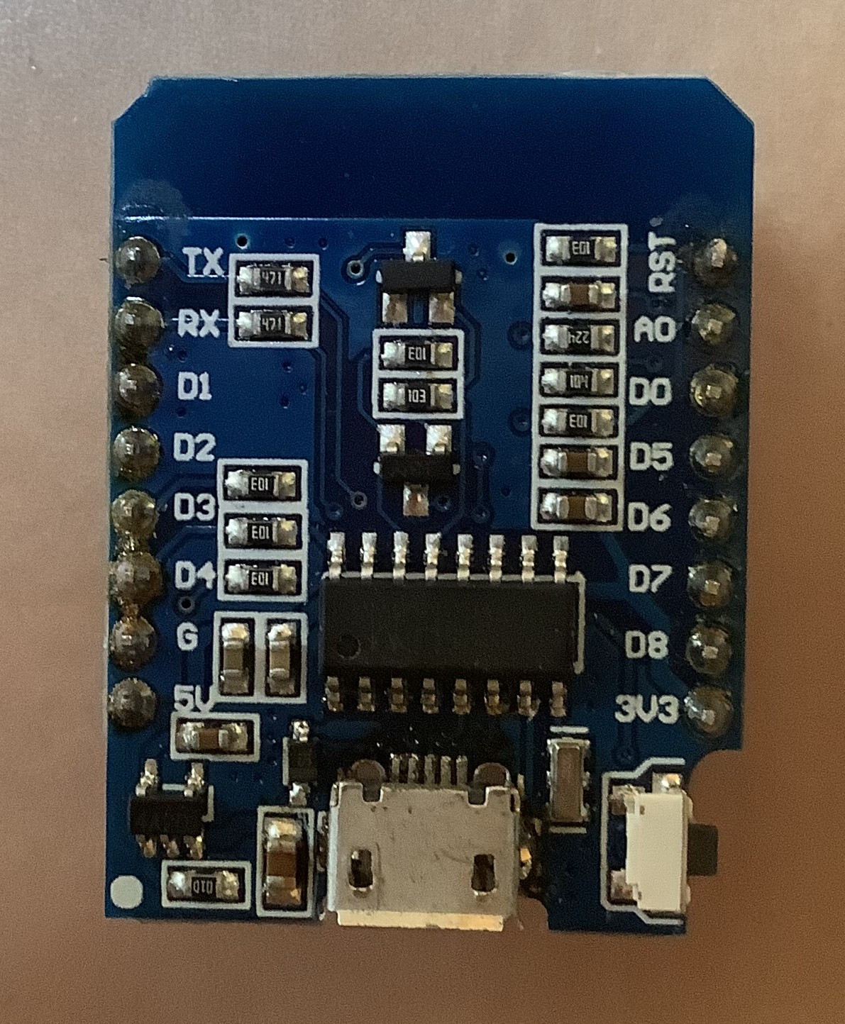
From left to right...
The LiPo voltage warning is generated by the comparator through the sense circuit R1, RV1 and R2 for a trigger at 3.2V. The output is going through a capacitor to create a negative going pulse that triggers the CMOS 555 timer. R11 and C5 create a pulse output of about 50mS, that needs to be inverted by an N-FET to drive the RST input momentarily low to wake-up the ESP. (I first used a transistor pair but was not happy about it and it also used quite a bit of power) I also have a voltage supervisor on order and may add that to the layout as an option. The comparator is one that I had left from another project, but you can use anything that fits the SOT 23-5 foot print.
So whenever the LiPo cell voltage is getting below 3.2V, a distress signal will be transmitted to the receiver, which in turn will switch on an LED so I can see that the LiPo needs to be swapped-out.
A cell voltage of 3V2 has enough head room for the voltage regulator to provide 3V1 to the circuits.
This section of the circuit is not yet implemented in the circuit that is now in the letterbox. It is still in prototype form on my desk (see below) because it's too finicky to implement that on protoboard. That will have to wait when I have fully tested the LiPo supply circuit and a PCB designed. More about that later.
The activation sensor that is fixed to the lid of the mailbox, should send a low pulse when the lid is opened. The position of a tilt sensor should be such that the contact is open when the lid is down, but shorts when the lid is opened. A vibration sensor will have a much less critical position on the lid, as it reacts on any movement of the lid. After quite some consideration and testing, the sensitive SW-18010P is the sensor that I decided to use.
The sensor creates a momentary negative going level on the RST input, waking it up for an "I got mail" message. This can be important when you use a tilt sensor and a larger package is stuffed in the mailbox that keeps the lid open. This 555 circuit will still produce a wakeup call. Without it, the ESP would be held in a permanent reset, and I would not get the "I have mail" message.
The LoRa board is connected to the ESP such that the ESP can initialize the LoRa board, and send or receive messages by using a software serial interface. That means that I can still use the Micro-USB or USB-C port to upload new firmware and monitor what it is doing by using the hardware serial port.
I added a reverse polarity protection and a fuse for the Lipo connection to prevent a possible to short of the LiPo cell or destroying the components on the board when the wires to the LiPo connector are swapped. I'm using a key'd connector, but not all cells have the same pin-out.
Whenever there is a mail alert, I also measure and send the LiPo cell voltage to the receiver. The receiver will react on a cell voltage that is deemed to be too low, so we don't need to wait for the distress alert alone. The combination will ensure that I detect the low cell voltage even when I don't receive mail for several days. If I get the alarm and both LED's are on, I need to swap out the LiPo cell.
Right now, for the prototype that is in the mailbox, I first used the LiPo cell directly to feed the 5V input of the WEMOS. That worked well for quite some time, but to get more mileage out of the cell, I temporarily installed a little boost convertor module that uses the LiPo cell as the input, and I adjusted the output for a 5V1 voltage, and that goes to the 5V input of the WEMOS so there is a reliable 3V3 to power everything. I did find that the Lipo discharged after about 2 weeks already, partially due to the cold weather, but I need to investigate that further.
I added the components for the receiver to this schematic, so I can create one PCB that can be used for both, to save cost.
Using a LiPo cell to supply power
It took me a while to figure out how to do it, because it's not so obvious. Let me explain.
Supplying the +5V input?
The ME6211C33M5G on-board voltage regulator on the WEMOS D1 (and the clones) that creates the 3V3 rail, feeds the ESP8266 module itself and in this design, also the LoRa module. This is a voltage regulator that, according to the datasheet, should have a 120mV drop-out voltage at 100mA and 260mV at 200mA. I measured that the 3V3 output starts to drop at an input voltage of 3V4, which confirms that. When the LoRa is transmitting however, the current will go up, and the drop out voltage will raise with it.
This limit of at best 3V4 by directly feeding the LiPo cell into the 5V input is reducing the usable capacity of the cell to about half, see the discharge graph above. I want to try to wring some more life out of it, thereby extending the time I need to swap it out.
Technically it works, but for this application it is a no for me.
Supplying the 3V3 input?
Can I use the LiPo cell to directly feed the 3V3 voltage inputs to the ESP and the LoRa module?
The ESP-12F module which is on the ESP8266 WEMOS D1 mini, has a voltage rating of 3.0-3.6V. The E32-433T20D LoRa chip has a voltage rating of 3.0-5.5V. It seems the LiPo cell voltage can drop all the way to 3.1V to have a bit of a safety margin.
Fully charged, the cell has a voltage of around 4V, which is too high for the ESP module.
So I can't use the cell directly.
Using the LiPo with a different supply option
Using an "external" very low-drop voltage regulator will be the answer.
This seems simple enough, but wait...
The problem to watch out for is going to be back-feeding from the 3V3 regulator on the WEMOS board when I connect the USB cable for debugging or uploading because there is no series diode or diode across the 3V3 regulator as protection on the WEMOS board. The USB 5V has a series diode to prevent back feeding to the connected PC, see below. I need to make sure that the regulator I'm going to use to power everything never exceeds the 3V3 of the WEMOS regulator. That should not be a major issue because my plan is to use a 3V1 supply rail to get more mileage out of the LiPo cell.
Eliminating the USB 5V back feeding into to the circuit
This is only an issue when you connect the circuit to the PC through a USB cable for testing or uploading new firmware. It does no harm, but will mess with the voltages on the receiver board, in essence lifting them up to 3V3. If you want to prevent that from happening, there is a fix. Here is the relevant portion of the schematic that fits most WEMOS variants. There could also be a 100K resistor from the EN pin to GND on some boards.
The 5V comes in through the USB connector and is fed through a Schottky diode (D2) to prevent back-powering the PC when you apply 5V directly to the WEMOS board. (BTW, I have never seen the 500mA fuse used on all the different boards I have).
In any case, the +5V goes to the 3V3 voltage regulator U1 and also to the USB to UART chips.
The three WEMOS variants I have use the CP2104 or the CH340C USB to UART chip. Even though the 5V is going to these chips, they function without it. I tried.
So the most simple solution for the USB power back-feeding into our circuit is to remove the series diode on the WEMOS board, which will prevent the USB supply to feed the 3V3 regulator. This Schottky diode is D2 on the schematic and can be easily removed. I removed it and applied 3V3 to 3V0 to the 3V3 pin on the board to power it and everything, including the USB serial monitor still works on both of these boards.
The location of the diode is pointed to by the arrow for one of my clones.
On the other clone with the CP2104, the diode was located to the right of the 5V pin and is already removed.
With the diode removed, there is no +5V going to the 3V3 regulator on the WEMOS board anymore, so a further refinement could be to also pull the +5V pin on the connector for the WEMOS board to GND, because that will also pull the EN(able) input from the 3V3 regulator down, and disable it. I tried it and it worked, although I did not test the back-feeding by applying a voltage higher than 3V3 and see if the regulator survived.
If you want to go really go fool-proof, you could also remove the ME6211 from the WEMOS board.
Using an external voltage regulator
While searching for a variable voltage regulator with a very low drop-out voltage, I found the TPS73101. The dropout voltage for this regulator is typically 30mV to a max of 100mV at 150mA, and only has 1uA current consumption which is all great. LCSC carries the part so I ordered a few of them which will arrive soon.
The output voltage of the regulator can be set by two resistors. I was planning to use 50K (2 x 100K parallel) and two resistors in series (27K+4K7) for a 31K7 value to set the output voltage to 3.10V, which is sufficient to power the critical components. The parallel resistance is 19K4 and very close to the recommended 19K. Due to the very low drop-out voltage, I'm planning for a 3V2 alarm, so I know it's time to swap out the LiPo cell for a fully charged one.
This also means that I can draw on the LiPo cell for just about the maximum 2000mAh capacity.
The voltage regulators arrived and to try it out in the prototype, I soldered one of them on a DIP carrier board. I then found out that the adjustment to get a precise 3V10 output with fixed resistors is too finicky. You would have to use three in series to get a precise output value so I'm now using a trimmer instead. That, plus some other minor value changes resulted in an updated version of the schematic above.
I took out the sender prototype contraption from the mailbox so I can test a few more things, especially to have a more detailed look at the current consumption. When I'm satisfied, I can start to create a PCB. The current plan is to create one PCB that will accommodate both the sender and the receiver to cut cost.
Change the on-board regulator
One alternative is to replace the on-board 3V3 regulator with a low drop 3V3 version. This will limit the available capacity of the LiPo cell to about 3.35V, but may be a viable alternative. The PCB that I am designing will support that option, you can just leave out the 3V1 circuit components and modify the software.
Current consumption analysis
Analysis may be a big word, but I tried 4 different ESP8266 board after I noticed that the current consumption in deep-sleep was much higher than I expected. I tried all four versions that I have with my prototype. It currently, does not have the LoRa module installed. That will be next.
Here is what I found, while powering the board with 3V2 applied to the 3V3 "output".
GY-D1MINI
This board uses the SIL2104 UART and consumed around 26mA when running in setup and 6.4mA in deep sleep. This is the one that I used on the prototype on my desk and the amount of current in deep sleep got me confused. It has the ESP-12F metal can module mounted on the bottom. It also has an LED installed that is connected to the UART, that cannot be turned off in software, at least I could not find how. There is a D2 on this board that can be removed.
With 6.4mA, this board has the highest deep-sleep current consumption.
D1 Mini clone
This board uses the KH340G UART. It is what I had in the letterbox. This board has the ESP8266MOD metal can module mounted on the bottom. It consumed 20mA in setup and 195uA in deep sleep. There is an unmarked D2 on this board that can be removed.
Apart from the WEMOS D1 Mini V4 below, with 195uA, it has the lowest current consumption in deep-sleep, about double the V4 board below, but that has another significant problem.
Unmarked D1 mini clone
It looks like this board uses the KH340G UART, but the markings are removed. It consumed 19mA during setup and 250uA in deep sleep. It has the ESP8266MOD metal can module mounted on the bottom. There is a D2 on this board that can be removed. Unfortunately, I can't find a schematic for this board. I wonder where the two large diodes just above the USB micro adapter are for.
WEMOS D1 mini V4
This board uses the KH340C UART. This board has a connector for an i2c interface and a USB-C adapter. It does not have the ESP8266 metal can on the bottom but uses the ESP8266EX chip. The board also has a 32Mb SPI flash chip and an ME6211C33 voltage regulator. According to the datasheet, it has a 100mV drop-out at 100mA.
The board consumed 19mA during setup and just below 100uA in deep sleep. This board has no "D2" installed, so the USB 5V always feeds the on-board 3V3 regulator when connected to a PC.
With 100uA, it has the lowest current consumption in deep-sleep, about half of the best of the rest.
A real gotcha with this board!
The major draw-back for this board is that it has a different pin-out. The pinout is actually flipped upside down compared to the all the other boards I have, making it somewhat of a tricky layout decision because you can only use the other boards mounted upside down. Compare the bottom markings with the boards above. All the other boards I have were always mounted with the USB connector on top. To do that with this board, you would have to mount it horizontally flipped to keep the RST pin in the upper right-hand corner, and adhere to the same layout. Strange, and a serious cause for a bad layout.
I also have an Adafruit HUZZAH but that does not have a USB connector and AI-THINKER modules which are larger, so are not candidates.
Removing D2, do or don't?
While trying all these boards, I found that there is no urgent need to remove the D2 diode, as long as the voltage rail of the letterbox sender is below 3V3, which it should. Just be careful when you are fiddling with this supply voltage and keep it below 3V3. What does happen when you leave D2 in the circuit and have the USB cable connected to your PC is that the WEMOS board will supply current from the 3V3 regulator to the receiver, and lift the voltage to 3V3. In that situation, you can't test the battery cut-out circuit or accurately measure the current consumption. Keep that in mind.
The overall current consumption of the circuit without the ESP or LoRa is 550uA at a cell voltage above 3.2V, and then goes up to 835uA when triggered. With the ESP at deep-sleep, the total consumption, still without the LoRa is below 1mA.
Just measuring the LoRa board by itself shows that when there is no activity, with the ESP in deep sleep, the LoRa board only draws 1.8 uA. When sending, it consumes at least 110mA in bursts for a very short time.
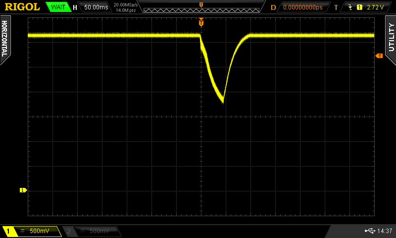
The screen shot below was taken through a 10R resistor in series with the VCC of the LoRa board, which is fed directly from the LIPO cell, to not produce voltage sags in the 3V1 rail, which could trigger a premature low batt alarm.
Luckily, I don't need to turn the LoRa board power off in the sleep mode.
Protection fuse
I initially added a 100mA PTC fuse in series with the LiPo cell, with an attempt to avoid serious issues that can be caused by connecting a LiPo cell. What you have to take into account however is the voltage drop over the fuse, the tripping voltage and the time before it trips. I'm not an expert at all, but it looks like a 100mA PTC will trip at 200mA and will take about 2.2 seconds before it trips. (this is the part I have and looked at: a radial RXEF020 from Littlefuse) It has a resistance of 1.8Ohm at room temperature.
In deep-sleep mode, the drop is only 1.3mV, but increases to almost 150mV during the LoRa transmissions.
That's quite a lot for this application, and I don't like the long tripping time, so I'm changing the fuse type to a fast THT Pico fuse of 250mA. Because I'll rather be safe than sorry.
Reverse Polarity Protection
The other safety measure I took was to add protection for a reverse polarity connection with the LiPo cell. I'm using a connector with a key, but not all LiPo cells come with the proper orientation of the wires. That can easily be fixed by swapping the leads in the connector, but you really don't want to have it wrong, hence the addition of a P-FET. The AO3401 has an RDSON of 60mOhm at 4.5V and 85mOhm at 2.5V, so it will be somewhere in the middle. The voltage drop of that device is not a concern.
Rail buffering
With everything connected and working, I looked at the power rails in more detail, because I noticed a sagging when transmitting.
It turned out that I had to use a 1000uF capacitor on the 3V1 rail, and another one on the LiPo rail that supplies the LoRa board, to reduce it considerably.
This is the 3V1 rail without any electrolytes:
One 1000uF added to the 3V1 rail:
Another 1000uF added to the LiPo rail:
This was taken with my Lab Supply with 2ft leads powering the prototype with 3V3.
When I switched to the LiPo that had 4V with very short leads, this was the result:
Obviously, this is with the prototype on proto-board, which is notorious for poor connections, but still...
Something to keep an eye out for. As a result of this observation, I've added a capacitor to the base of the voltage trigger transistor, with an attempt to not let it trigger on a sagging of the rail during transmission.
There may be a potential issue with the power-up of the ESP due to this added capacitance. The chip will go through a voltage ramp-up that may cause instability. I will look at that later in more detail, but right now it does not seem to be an issue.
Update: When I looked at the rails again with the PCB version, there is no more sagging. There is still a lot of hash just about everywhere when the LoRa module transmits, but that seems to cause no harm.
With the design pretty much done and functioning pretty well in both hardware and software, I started to design a PCB, and I used a board outline based on the Hammond 1593L enclosure I want to use.
However, while thinking some more about the consequence of adding the large electrolytes (or a super cap) on the power rails, and the potential start-up issues for the ESP (it spends some time in the unstable zone due to the slower voltage ramping up), I considered using a voltage supervisor. This chip would keep the ESP in reset until the voltage is stable. While looking into possible candidate solutions, it dawned on me that I could use one as a cell voltage alarm, and eliminate the two transistor voltage sense circuit. Alas, I did not find any with a trigger voltage of 3.2V, and only a single one with an adjustable input that is more or less commonly available, the NCV308MTADJT1G or the equivalent NCP model. I ordered two NCP versions and will try them soon. This chip draws only 1.8uA, so is a significant enough improvement on the power budget as well. Because I was not happy with the two transistor trigger circuit, I redesigned it using a comparator. I will try to add the layout for the voltage supervisor for the trigger so it can be used as an option. When I have the PCB, I can better determine if I need the extra electrolytes and also if the ESP will experience power-up issues.
Initially, I was planning to set the 3V2 trigger level with resistors, but after I changed the resistors to much higher values, I did some calculations for the proper values and decided to make it easier, albeit with the expense of another trimmer.
The above schematic is what I used to the create a PCB. It has the optional MCP308 voltage supervisor chip that can be used instead of the TS881. Note that I'm now using the WEMOS D1 mini V4 that KiCad supports but with the flipped pinout, because it has the lowest current consumption. Other WEMOS D1 boards can still be used when they are mounted upside down.
The same board can be used for both the sender and the receiver. Several parts can be omitted or added to suit either version.
When I received the boards from PCBWay, they looked perfect as usual. The position of the drilled holes is exactly where they need to be, I always look for that as a quality indicator, and the silkscreen is crisp.
Spoiler alert: I successfully reflow soldered the boards on my new hot plate prototype. That is a project that has been under development for a while, in parallel, and I will start a Blog post as soon as I finish this project.
I build the sender version and started to test it out. The 3V1 adjustment is a little sensitive but easy to do. After having done that, I could now also adjust the 3V2 cell voltage alarm setting. I used a power supply instead of the LiPo cell, so I could finely adjust the voltage and set RV1 to a 3V2 trigger point.
When I then tried the sensor to activate the mail alarm, I noticed a goof in the schematic and subsequent layout. The sensor input is going to the wrong end of C2, meaning that a tilt sensor would continue to keep the 555 timer and the RST signal for the ESP low, not allowing it to boot if the mailbox lid stayed opened due to a large package. I cut the trace and used a small wire to attach the signal to the "right" side of C2, and that worked well. Of course. But that also got me thinking. A tilt sensor has to be positioned a little slanted to make the contacts short when the lid is opened. The lid opens just above 90 degrees in a normal opening position, and about 160-170 degrees when fully open. I was envisioning a 45 degree angle, with the sensor upside down in the open position, which is what I used with the mercury switch as well.
However, when you use a vibration switch, this all does not matter. So after quite a bit of testing and contemplating, I decided to use the sensitive SW-18010P sensor. I modified the layout to accommodate this change so that will be on the GithHub, making the board more universal.
Below is version 2.3b that incorporates this minor change.
When I tried to activate the LoRa module, I was seeing weird behaviors. It turned out that I made another layout mistake and swapped the board connector 180 degrees. I fixed that for my two modules by removing the connector from the boards, and soldering a new connector to the other side so I could mount the boards upside down. The layout error also has been fixed and is below with version 2.3b.
With this board, I used the TS881 comparator, not the MCP308 voltage supervisor.
When you think you are done...
When I further started to test everything, I ran into a few more issues. First of all, the comparator worked really well detecting a low cell voltage, but caused an oscillation during the low bat condition. When I applied 3.2V, it triggered but also resulted in a continuous reset of the ESP at this voltage. The rail goes up and down a fraction when the ESP is awoken and the LoRa module transmits. I hoped that the disabling of the 555 timer by software would prevent this, but it didn't. The normal practice is to add some feed-back to the comparator to create a hysteresis, but with the high value resistor values I selected to cut down on the current consumption, this would need to be in the 100M+ range. I don't have these values, and it also really messes with the resistor selection.
So, it was time to activate the optional voltage supervisor and see if that would improve matters. The NCV308 has an internal hysteresis, so that should help. I calculated a workable set of resistor values and changed the circuit on the PCB and gave that a try. Presto, problem solved! This is a much better solution.
Next I also experienced strange reset issues with the ESP modules. Some of them need a very long reset time, at least 5 seconds. At first I didn't know this, but after some Googling I found that this is normal. This reset issue is unrelated to the voltage rail capacitors on the board. It's just the way it reacts to pressing the on-board reset button. This was kind of strange and unexpected for me, because the other ESP modules I tried earlier had an instantaneous reaction to the button, or shorting the RST pin to ground to wake it up from deep sleep.
The result of a too short reset pulse was that although a mail or low cell voltage was detected, the WEMOS D1 mini V4 did not fully reset and restart. It did something, because I got some weird characters on the serial monitor (due to the used Baud rate by the kernel). That problem was solved by changing the 555 timer setting to produce a more than 5 second reset pulse.
And then, I suddenly, out of the blue ran into a myriad of issues (error messages) when I was trying to upload new firmware to the ESP boards. After a lot of searching and head scratching, I figured out that the CH340 driver that is needed for most ESP boards has to be an older version than what I had installed. The latest driver will not work properly with these cloned versions of the CH340, and will give all kinds of communication errors. I had fixed that issue a very long time ago, which is why I couldn't figure it out at first. It turned out that the older driver that I installed a long time ago and worked, got automatically(?) updated to a newer version. Be aware of this issue, it cost me several hours chasing it down. The older version number for the driver that works for me is 3.4.2014.8 and has a date of 8 Aug 2014. Here is a site with a description of the issue and where you can get working drivers:
older CH340 drivers.
Because the WEMOS D1 mini V4 had more serious issues with the reset duration, and I also was struggling with the serial port, I tested some of the other ESP boards that I have. Eventually I picked one that did not have the pins soldered in yet, so I could mounted it upside down in the circuit. It worked well, so I just left it there.
To accommodate boards that have this 5s reset issue, I selected the timing components for the 555 timer to have at least a more than 5 sec reset time, using worst-case component tolerances.
Finally, I ran into mysterious reboots when I thought everything was working. It turned out that the sensitive vibration sensor version (SW-18010P) is so sensitive that it continuously activated the trigger circuit and restarted the ESP. It was just lying still and untouched on my desk and still produced random triggers. The very fast needles it produces are very hard to see on the DSO, and I simply missed them for quite some time. Replacing the sensor to the less sensitive version (SW-18020P) solved that issue as well.
So finally I got a functioning receiver and a sender.
To the left is the sender that will go into the mailbox. The lower right white connector is for the sensor, and the upper right one is for the LiPo cell. This board has the WEMOS D1 mini clone installed in the upside down position.
The receiver is on the right, and only has three resistors soldered on the board for the LED's and the reset switch. They connect to the bottom three connectors. Two polarized white ones for the LED's and the middle one for the reset switch. The black round device is the beeper. This board currently has the WEMOS D1 mini V4 installed.
Final current consumption
With everything working and populated, it was time to do another power consumption analysis.
I applied 3.6V to the sender board with my power supply and measured the current with my DMM.
With both the WEMOS D1 mini clone and the LoRa module added, the total consumption is 1.07mA with both modules in deep sleep mode. With the WEMOS D1 mini V4, the total consumption dropped to 940uA. This is higher than I hoped for, but the best I can do. I'm going to keep the clone installed for a longer testing period.
My assumption is that with a 2000mAh LiPo cell, I would get enough time in-between charges. Time will tell.
The sender is installed in the mailbox and the receiver is on my desk so I can try it out for a few days.
Fitting it in mail box
The mailbox lid sensor types you can use can be two-fold, depending on your mail box and more importantly, the lid.
Below is a picture of my mail box. The lid is positioned at the top and swings outside to just below 90 degrees. This is a problem for most switches because they may not react well, so you need to position them at an angle. I experimented a lot, even tried the tilt switch with zirconium magnets that would lift the luckily magnetic balls inside the switch free of making contact. However, I did not like that construction at all. I needed several magnets, and they were glued to the lid. They stuck-out too much, and could be broken off when the mail is inserted.
The challenge I have is that I don't have much room, and the construction is severely limiting my activities. Just below the lid is a ledge of about 2 cm, so I can't really position anything below the lid. That would be too easy.
After many attempts, I decided to go back to using a vibration sensor, that is attached to the lid. When the lids drops down into the closing position, it should jolt the vibration switch enough to give me a reliable signal. I contemplated using the sensitive version, and I tried it, but that one is really too sensitive. I suspected that a neighbor ledge dropping down could already trigger mine.
The actual sender enclosure is taped with double sided foam tape to the front of the mail box, There is a ledge above it of about 1.5cm that protects is from heavy mail dropping on top of it. Initially, I located the sender and LiPo in the back of the mailbox, but a large box that was forced into the mailbox, dislocated the sender, so I now moved it to the front. The cable going to the sensor is now too long, so I should shorten it and move it out of the way of the antenna. But, it is working fine so far, and I added the cover of the enclosure box.
There is a short extension cable between the PCB and the LiPo cell. I used that to make the exchange of the cell easier, because it's not so easy to put the plug in when the enclosure is where it is and the cover is on.
Another (last?) improvement
Depending on the sensor type, you need to connect them on either side of C2. When you use a switching type, because it can stay open with large packages, the signal needs to go through C2. Vibration switches on the other hand produces pulses, not a level, and they can be connected either way of C2. I modified the schematic and now include a solder bridge so you can select either type.
The updated schematic and layout
A real gotcha!
While I was testing, I ran into all kinds of seemingly spontaneous triggers, and worse of all, the system would get into a reboot cycle and never went to sleep. So I did not get the mail message, and the cell was draining fast. After a lot of trying and testing on my bench, it would 99% of the time work fine, but as soon as I travelled the 3 flights of stairs down and installed in the letterbox, it would 100% fail and reboot all the time. I traveled up and down the stairs a lot trying to figure it out.
Because the sensor is mounted on the lid and the leads are going through a small plastic conduct, I would leave that in the mailbox and just took the enclosure and the LiPo cell with me. When I was testing it on my bench, I would simply short the input connector the simulate a trigger. It always worked so I could not find the root cause of the error.
Eventually I got so frustrated that I ripped the sensor with the wire out as well, and put that on my desk. Then I had a hunch that the transmission signal could enter the sensor leads, and indeed, as soon as I wrapped the leads around the antenna a few times, I could verify the reboot problem. The solution of course is to use shielded cable so close to the antenna. When I did that, the problems went away. Keep that in mind.
Testing it out for another week showed no missed mail and it works great.
I have now created a new project on my Github, and put all the information in there. If you think something is missing, leave a message. The details of the project can be found here:
Github
Note that when you upload the Gerber files to PCBWay, who is sponsoring this project for me, you'll notice that the Gerber viewer in the upload section does not fully show the picture. When you use their online Gerber viewer, it works fine.
I also created a so called "Shared Project" on the PCBWay website that can be used as well.
Conclusion
We normally don't get a lot of mail, sometimes days without anything, but in the current busy Christmas period we get mail all the time, and the prototype was functioning very well. When I took it out of the mailbox and started to work on the PCB's, we really missed getting the "I have mail" message, that we so quickly got used to it. This is a keeper!