
I started this post in December 2017 on what I now call the Version 1, which was actually a working prototype. In January 2021, I blew-up (through my own haste and stupid fault, I connected an incorrect external transformer) my Curve Tracer (CT) and damaged so many parts that it is difficult to get it back to where it once was. There are a number of reasons why I have decided to build a new one. A follower of this Blog has used my design to build PCB's and made some enhancements to what I now call Version 2 and others are following, so there seems to be a growing interest in this project. I'm also soliciting the help of others to critique and help design Version 3, which will be based on Version 2. Send me a message below if you want to be on the V3 team. The new version should have more features, will be more robust, easier to build and be optimized as much as possible for the DSO display medium.
This blog will now be used mostly to describe the Theory of Operation of a Curve Tracer, and describes the building of my first version.
Version 2 has now it's own Blog here : Version 2
It also has the detailed information for the circuit diagrams, the BOM's, the PCB's and some of the issues we've identified.
The Version 3 Blog can be found here: Version 3.
It will have the details for the hopefully final version.
===========================================================
As I mentioned in an earlier post, I sold my DIY Tektronix analog mainframe scope, and with it, my DIY 5CT1 Curve Tracer. That project is also described in yet another post on this Blog.
Why I want a Curve Tracer
It's not that I use a Curve Tracer that much, but if you want to categorize or really measure the parameters of a discrete active component, there is really no other tool that can do the job well. Of course, there are very simple tools and gadgets available that do a go-no-go test, and even can give you the current amplification factor. I have one of those too, but they are very limited in what they can do. It's also fun to design something like this, as a mental exercise, which is why I do a lot of these things. I like to design and build Test and Measurement tools.
With that in mind, I started a project in early 2017 to build my own Curve Tracer, not unlike the one I already had, the Tektronix 5CT1 that I built in early 2000. Information about the 5CT1 can be found here : http://w140.com/tekwiki/wiki/5CT1N
By the way, the 5CT1N (the N stands for no parameter readout. I modified mine to add that, which is why it is probably the only one in the world without the N suffix. This CT is also known as the 7CT1N. That instrument is really a 5CT1N. The only difference is the adapter board that changes the mainframe connector from a 5000 mainframe to a 7000 mainframe.
Even the 5CT1N or the equivalent 7CT1N plug-in CT unit, that I build almost 10 years ago myself, is not easy to replicate in a DIY project, but we
can come pretty close.

My ca. 2002 DIY replicate.


The Scope of the DIY CT Project and Why
In the course of looking at more modern designs (the Tek 5/7CT1N was designed in the 1970's) I found about a number of different implementations and architectures.
There are two main architecture types.
One of the architectures uses an Arduino or another micro controller to drive the hardware settings and then collect the data. They typically use a PC as the display, or an LCD/OLED type display.
I skipped that architecture type right away because to me this is the least "real-time" method of using a CT. When you are
profiling a device, you want to have immediate feed-back from your
adjustments to see the results and to also prevent blowing up the part
when you apply too much current or too high a voltage. DUT's can be very easily killed in seconds by the hands of the operator due to a thermal overload.
The other architecture type uses the truly or almost real-time display of the results.
Analog display types (CRT based analog scopes) are truly real-time, DSO's are almost real-time. (explained below)
Of these, the ones I found are all variations on the same, more traditional theme.
Apart from the Tektronix 5/7CT1N, 576/577 types, four really standout.
The B&K 501A was a simple but complete instrument dating from the 1970's : 501A manual download
The 501A is a testament of what smart designers could do with the minimum amount of parts.
One is the Heathkit IT3121. A Manual and schematic can be found in this archive :IT3121
Another one I'll call the Changpuak version, and details can be found here: Changpuak
The last one is the ELV KS7000. You can see a demonstration of it here : KS7000
The ELV units were available as DIY kits a long time ago, but these kits are no longer available. The ELV 7000 is more modern (around 1985) and has a few nice features that to me are important. I'll cover that later. The Heathkit IT3121 and the B&K 5-1A are almost a copy of the typical (traditional) Tektronix Curve Tracers, which are, in my opinion, the de-facto standard in Curve Tracers, the 576 in particular. I used to know that marvelous instrument very well. When I was at Tektronix in my early career, I used it a lot while hunting for bad or failed components for a number of years while I was repairing Tek equipment in the mid 70's. The Changpuak one is also well documented, and the most modern one, but to me, lacks some critical functions.
However, let's put this project into a little perspective by looking a bit at the top of the line vintage instruments, the Tektronix 576 and also the 577 because they are still in use in many places.

This is the inside of a 577, using a 5000 mainframe. A very complete, very precise but also very complicated instrument!

Duplicating a professional instrument like these top of the line CT's is not possible with a DIY project, of course, but it shows the enormous complexity of these instruments.
The Trade-Offs

Here is a typical result, taken from my DIY rebuild 5CT1 in my DIY rebuild 5440 mainframe:

The top readout (100uA) is the Collector current (IC) per division, and the lower readout (2uA) is the current per step (IB) fed to the Base. These are the unique read outs that I added to my version.
From these curves and the readouts you can deduct, calculate or measure the Beta or current amplification in the common Emitter Mode (IC is approx. Beta * IB), and look at the linearity, the voltage breakdown and temperature drift among a few others parameters.
Look here for an explanation of Hfe/hfe/Beta here : current-gain-hfe-beta
The Advantage of the Analog Scope/CRT
In the "old" days, the scope or display was an analog scope with a phosphor tube. The phosphor was relatively "slow", meaning that the trace glowed for a short period. This feature allowed the Curve Trace designers to use the mains frequency of 50 or 60 Hz. As you can imagine, the repetition rate of the X-Y trace is depending on the number of steps coming from the Step Generator. With a typical 7-8 steps, the repetition rate of the sweeping phosphor trace is 50 or 60 Hz, multiplied by 2 because of a diode bridge to get positive or negative excursions, and then divided by the number of steps. The more steps, the more the display starts to "flicker". The so called "re-trace", when the X-Y beam is rapidly moved from one place on the screen to the next, is so fast that the phosphor does not light up, or if, only a little. This feat was thankfully used by the Curve Trace designers, it made for a relatively clean and sharp picture.
A downside of this design, used in the 577, was that the used half sine wave for the collector supply, as coming from a mains transformer, showed a trace that was "thicker" or with a higher brightness at the top of the sine wave, or at the end of the horizontal axis, when the beam travels slower. The 5/7CT1N uses a triangle waveform, so this effect is absent, as you can see in the picture above.
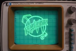
The Pitfalls of using a CT with Digital Sampling Oscilloscopes (DSO)
With the advent of digital scopes, the X-Y display feature changed dramatically. Gone are the days that you could deflect a single beam in a CRT (Cathode Ray Tube) to any of the X-Y axis coordinates at will and in real-time. Displaying the trace in addition to the readout of the settings in my CT in the picture above, and the crisp display of the vintage Tek logo (on an HP scope) are a testament of that feature.
The down-side of this method is that you are completely depending on the repetition rate of the X and the Y signals. If you use a scope with two channels in the X-Y mode, you can still control the Volts/Div settings of both signals, but not the timing.
Digital scopes in the X-Y display mode sample both the horizontal and the vertical channels and store the values in the acquisition memory. When that is full, the processor calculates the recorded values as X-Y coordinates to display on the screen. The process is repetitive but no longer real-time and it also results in a fairly to sometimes a very fuzzy display, because the "trace" is really a scattering of collected samples, that cannot be converted to a line anymore. This display method knows nothing about retracing, so it displays everything captured, with the same intensity.
There's no hiding anything anymore. What you see is what you got, or in another way, what you got is what you see. Gone are the CRT advantages the "old" Curve Trace designers relied upon.
However, the good news is that with a DSO, you can still control a number of things in the X-Y mode. You can select the depth of the acquisition memory and that will influence the time it takes to fill 'er up. You can also still change the time-base and that will determine the number of samples per second, and that determines the composition of the trace with more, or fewer samples per say displayed inch, and also the repetition rate.
Another significant feature that a DSO has and an analog scope doesn't is the ability to easily make screen shots of the display, and they can even include the settings which is great for documentation purposes.
I recently purchased a Rigol DS2072A, and although I really like the scope in normal operation, the X-Y display in the default mode is disappointing if you're used to a cathode ray tube. It's not full screen, because that would make the scattering even worse, and without adjustment, the picture is dim and not very appealing.
Here is what I mean:
I used the following two CT related signals that are fed into the two scope normal vertical inputs in the normal time base mode.
These two signals show the principle of a Curve Tracer (CT). The triangle waveform is the voltage applied between the Collector and the Emitter of the DUT. The Base (current for a BJT) or Gate (voltage for a FET) as shown here is driven with a stepped waveform. The step heights will drive the FET with increasingly higher voltages. In this particular case, there is one half (either up, or down) of the triangle waveform for every step. We'll cover that and other options in more detail later.

Below is a picture of the Step Gen output now put in the current mode for BJT's and that will result in the following picture for a 2N3904 transistor as the device under test (DUT).

When you put the scope now into the X-Y display mode, you get the following picture.

This was made with the default highest memory depth of 28 million points. There are so many points (samples) that when transferred into the X-Y coordinates, it almost looks like there are lines. The problem is that it takes time to fill the memory, and that slows down the repetition rate of the display. It's also too fuzzy and very dim. Also note the connection of the traces on the right-hand side. An analog scope will not show them, because it operates in real-time, and the phosphor is not fast enough to show the fast transitions, unless you really turn-up the brightness. This display shows the path of the steps in correlation to the triangle waveform very clearly.
You can tune the DSO display by using a lower memory depth, and I typically use 7K as the maximum. Note the much better display. The result is also a much sharper picture and will also have a faster update rate. You want it to be as fast as possible to react quickly to changes. Further tuning can be done by setting the brightness and adjusting the time/div speed of the time-base for the best picture and fastest update rate.

In the above two pictures, for every step, there is one half of the triangle slope. The triangle slope travels in the horizontal axes, the steps in the vertical axis. The origin is in the lower left hand corner of the picture, the cross-hairs of channel 1 (horizontal CE voltage) and channel 2 (vertical IC current).
The first step with the first half (positive going) slope of the triangle is the first horizontal line in the picture, starting from the origin on the left to the right of the screen. The second step, with an increased step value, will now origin a little higher on the right hand side where the first step ended and then travel back to the origin with the down going slope of the triangle. The jump is very fast, so on phosphor tubes, this will not show up at all. On DSO's however, the sampling will catch some of this travel as you can faintly see in the picture directly above because there are some dots with the limited sample depth of 7K. Remember, a DSO shows all the collected samples as coordinates while in the X-Y display mode, so it cannot "connect the dots" although it seems so when you use the maximum memory depth. The third step will start in the origin, and travel up to the level of the third step, and then horizontal with the triangle slope. The fourth step will jump up and then travel back to the origin.
An analog scope will "paint" the same trajectory in the fosphor with the beam following the same excursions in real time in exactly the same order as I just explained. Apart ftom the prossesing time-out a DSO needs, there is no difference, which is why you can use both scope types with this technology.
The travel from the traces on the left hand side going up are visible on the display, and is caused by the physics of the transistor (the approx. 0.6V junction barrier before the device starts to conduct).
Furthermore, this is a bit of a fuzzy display due to the display process of showing the coordinates of all the collected samples in the X-Y mode, and this is under almost ideal conditions. If the signals are smaller, the noise will increase, also a typical pitfall for DSO's, and the traces will be getting even more fuzzy.
This picture above was "tuned" to improve the visibility. With my Rigol scope, the "dimness" of the trace can be changed by the WaveIntensity setting, which by default is set at 50%.
Traditional CT's can use a saw tooth, a full triangle waveform per step, or even half a sine wave derived from the mains voltage instead. In those cases, the waveform travels back and forth for every step. In the case of a sine wave, you can imagine that there is an intensity difference if you consider the different rise times of those wave forms. The most optimum wave form in my opinion is really the triangle one.
Using a saw-tooth or triangle waveform based CT requires a special voltage regulator, a sine wave based CT can simply be created by using a half-rectified mains transformer secondary winding or taps.
The main take-away point from this section is the caveat that is typical for DSO's in the X-Y display mode. It's almost real-time and constructs the I/V picture differently. The screen is updated with the rate of the acquisition speed to fill the memory and also the calculation portion before the results are shown on the screen. There is a slight but natural flickering of the screen based on this repetition speed. This flickering is depending on the acquisition speed and memory depth plus the calculation speed of your DSO, and so will vary between makes and models.
What can be done to improve this
In order to try to overcome the limitations of a DSO as a capture and display medium, we need to take that change in architecture into account in the design for a Curve Tracer. Note that this is true for any sampling method, and that includes AD convertors with a processor like an Arduino, or feeding signals directly to a PC through a Sound Card digitization, etc. Most of these types are a lot further removed from real time which is why I abandoned these architectures.
Because of the almost real-time displaying of any digital sampling method, like a DSO uses, the display no longer "flickers" due to the mains frequency limitation of 50 or 60 Hz, but this is replaced by the acquisition processing rate. The only cure is to go away from the mains frequency timing relationship so we can increase and tune the triangle and Step Gen frequency of the CT to optimize that to the refresh rate of the used scope. This will require some experimenting because all digital scopes are different in that respect. Factors like sampling speed, memory depth, processing speed etc. all play a role.
The acquisition rate of the DSO can also be influenced by the Time/Division setting, even while in the X-Y display mode. You can experiment with the most optimum setting so you have the fastest update rate, without an annoying flickering caused by the time out "holes" in the display that are the result of the time needed for the digital sampling and processing.
When you abandon the mains frequency as the driving factor, you can also change from a half sine wave to a saw-tooth or triangle waveform. I experimented with a couple of different wave-form's, using my Function Generator, and I decided to settle on a triangle waveform. The major reason is actually that it is a lot easier on the Collector voltage regulator to handle a triangle waveform. Also the synchronization of the step generator with the triangle waveform is a little easier to realize. This is important because as I alluded to earlier, the digitizing method of a DSO is much less forgiving on timing differences and glitches or aberrations at these change-overs, and will display all of that.
Another decision that needs to be made is how the triangle waveform fits into each step of the step generator. You can imagine that you could have one rising edge on step one, followed by a falling edge on step two, followed by another rising step on step 3 and so on. This will insure that there is only one single "trace" per step, because when there is the slightest difference in the slopes or timing, you will increase the fuzziness of the horizontal display "trace" portion of a step.
Here is what I mean.
In the two pictures below, we now have a full triangle waveform for every step. Note that the first horizontal portion of the step goes up slightly, which is the result of the higher IC current due to the increasing Collector voltage. When the triangle waveform changes to the down going slope, there is a little jump in the middle of the step, after which the IC current goes down again, as a result of the lowering of the Collector voltage. I suspect that the little jump comes from a timing difference (propagation delay) between the Collector voltage output and the Step Gen output. There is also a small difference in the flatness of the step curves that can be attributed to the self heating and cooling of the device. These temperature changes will cause small changes in the gain of the transistor, and therefore the Collector current.

When there is the slightest difference in the IC current caused by the triangle going up or down, it will create a double trace which shows up as a thicker line. The curves do not really overlap each other. Gone however, are the jumps on the right hand side of the display.

Due to this "blossoming" effect on the traces, I decided to select a single ramp per step. In my design however, you can easily switch between the two modes, by just removing a single capacitor in the Step Gen trigger circuit.
When the DUT gets really hot, you could get an increased effect of the curves not overlapping anymore and this is called "looping" of the curves.
With this as an example, let me stress again that for a CT with a DSO as the display medium, the precision of the triangle wave form timing and linearity in relation to the stepped waveform and its timing together with clean edges and to top that of, the reduction of signal and acquisition sampling noise is crucial to get a clean display.
The Importance of the Step Generator
The take-away from all this is that especially the Step Generator design is much more critical than in the previous (analog) designs before.
Using the ELV design as the Blue Print
The ELV KS7000 design comes pretty close to fulfilling my requirements, unfortunately, that design was made at a time when FET's where not main-stream, and adding that capability to the design seems to have been an afterthought, and in my opinion, rather poorly implemented.
Furthermore, the Achilles-heel of a re-build of this particular design is made difficult because of the special transformer that were custom designed for this instrument. I already went through something like that with my own 5CT1 re-build, where I also had to call in help to produce a special transformer. Luckily, the ELV challenge can be solved by using multiple transformers.
The KS-7000 description and schematics are available on-line, unfortunately, it's all in German and you need a German address to satisfy the ELV demands on their website before you can purchase and download the two articles. I managed to purchase and study the documents, but I'm not going to publish nor send it to anyone, so don't even ask, please!
Although I based my design for a large portion on the KS-7000, which is no longer available in kit-form, I added enough changes and improvements so I can hopefully show my design here without causing issues.
Simulation and Verification
At this moment I should probably mention that I used
LTspice to simulate 5 different CT designs before I settled on the ELV one as the basis for my developments. I also build a prototype of a couple of the circuits to learn more about the pitfalls in the real world, and I actually built the complete ELV design as a working prototype.
Here is a picture of the 4 major components:

The box in the upper left corner is a simple adjustable supply I use
when I bread-board, and it is used to power the Step Generator with +/- 15V
DC. This supply needs to be floating from the rest as you will see later. Below it is the Step Generator, already with some of my changes and redesign. Below it is the Triangle Waveform Generator and the simplified Collector supply regulator. The collector supply output voltage can be varied with the potmeter below it.
Upper right is the power supply for the Triangle Waveform Generator (+10V and -5V). I'm using LM317 and LM337 for these supplies to be able to change the voltages in this prototyping phase. The Collector voltage itself was coming from one of my Lab supplies.
Lower right is the circuit for the X and Y amplifiers that interface to the scope X-Y input channels.
When I took this picture, the boards were no longer inter-connected to each other anymore. When they were, it was quite a display of wires and the whole thing looked like a giant spiderweb.
The Theory of Operation
----------------------------------------------------------------------------------------------------
I need to point out that I use my schematic capturing program (DipTrace) now only to show the Theory of Operation.
My diagrams on this Blog are no longer intended to be used to create a working instrument. The complete schematics and board layout information is available on the following Github site: https://github.com/markallie/Pauls-Curve-Tracer and described on a separate Blog here : http://www.paulvdiyblogs.net/2021/03/building-curve-tracer-v2.html
The part numbers and most values I show in the diagrams below could have no relation to the real schematics anymore.
------------------------------------------------------------------------------------------------------
After discussing the differences between DSO's and analog scopes and their pros and cons in the previous section, I'm now going to describe the full functionality of a working Curve Tracer with the above in mind.
While describing the functionality, I'll focus on a transistor as the DUT, but you can also replace that with a FET or other active components. The only difference is that a transistor needs a Base current, and a Fet a Gate voltage. This is one of the functions of the step generator.
Here is the most simplistic block diagram of a Curve Tracer (CT), where the shown transistor is the Device Under Test (DUT):

The measured collector current (A) through the transistor (actually the IC) is going to the X-axis of the scope, and the voltage (V) (actually the VCE) is going to the Y-axis of the scope. To display the relationship, the scope needs to be set to an X-Y display mode. These two (vector) signals together produce the typical curve tracer diagrams.
The Collector supply.
Because a triangle is the optimum waveform for the Collector supply, we need a dedicated supply. A mains transformer supplies the unregulated voltages that are required to create the regulated and adjustable triangle waveform that supplies the Collector/Drain voltage and current.
We'll start with the unregulated voltage supply that we will use to create the Collector Supply voltages.
To play it safe and use different kinds of transformers, we will use a setup by which we can select lower voltages and also higher voltages. This can be accomplished by simply putting the supplies made from the two secondary windings in series and use a relays to tap either one.
There is however a difference in the circuits for different types of transformers, or combination of transformers, you need to be aware of.
Both transformers in the above picture can be used with 115V mains as well, just put the primary windings in parallel.
If you use a true center tapped (CT) transformer, you could use one bridge rectifier, and use the traditional center tapped circuit but instead of a differential +/- supply, use the minus supply as ground and the middle will become the low supply and the top the high supply.
However, you cannot use this circuit for transformers with different windings, or two transformers with different windings. You will get unexpectedly high voltages due to a strange phenomenon that is a "real trap for young players". We got caught in that trap too when we tried the asymmetrical transformer in the circuit for a CT transformer! Mark Allie simulated this effect and came up with this explanation for asymmetrical transformer windings:
The non CT transformer arrangement seems to always go to the High DC for both halves of the bridge output. It turns out that the bridge rectifies the higher voltage while rectifying the lower voltage on the other half of the bridge and vice versa. So in effect both DC's see a low contribution and a hi contribution. You will see the DC be high until too much current is drawn and it pulls the high supply down where the low can offer more current.
Don't try to save on the extra bridge!
Note also that with the asymmetrical transformer and the two bridges, you cannot tie the transformer windings together at the AC side, to "create"a center tapped transformer! If you doubt this is possible, connect a DMM in the high current mode between the two center windings (S2 top, S1 below) and you'll see a rather high current flowing, and maybe hear the transformer sing a tune. You have to connect at the DC side of the two bridges.
Also note the "bleeding" resistors across both raw supplies. They make sure the rather high voltages are discharging relatively quickly. We will use a relays to select between the two voltages and use another one to also create different current levels for the supply.
Normally, you would switch the AC signals because relays contacts can withstand higher currents with AC wave forms, compared the DC wave forms. In this case however, I figured that's not a good idea, because when we gradually increase the Collector voltage for the DUT and reach the tripping point, there will be an inrush of current to charge the capacitor, potentially disturbing the measurement. We don't want that to happen so the capacitors are always charged. In hindsight, that decision caused other problems.
Below is a minimal diagram showing how we regulate and adjust the Collector Supply.

This circuit looks very close to that of a DC regulated lab power supply, and it indeed uses the same principles.
On the left-hand side, the unregulated DC supply comes in. We use a series power transistor to do the actual regulation for us. This Darlington type transistor has a bias current applied to the Base. This is accomplished by resistors R403 and R405.
The voltage level regulation is controlled by the Opamp on the left. The non-inverting input is fed by the reduced voltage from the negative side of the unregulated supply, through a potentiometer. The Opamp will set the output based on the differential voltage on the inputs. The output of the Opamp will draw current through the LED, here doing double duty as a diode, taking the bias away from the Base level of the transistor when it is in voltage regulation. This will reduce the conductivity of the transistor and regulate the output voltage based on the voltage that the potentiometer applies to the Opamp. The potentiometer can regulate the output voltage from zero to the maximum of the unregulated supply voltage minus the drop over the transistor.
To protect the DUT, we want to have a form of adjustable current limiting, analog to that of a lab power supply.
The
Current Limit is determined by the voltage
difference measured across the CL shunt resistor, between the transistor and the output terminal. The current limiting potentiometer determines the tripping point from voltage regulation (CV) to current limiting regulation (CC).
Creating a Current Limit for the DUT
There actually two ways of creating a current limit for a CT. The most common method is to use a large set of resistors and switch them in series between the supply and the DUT. You can easily see the result of this method:

Note that with higher step currents, the collector supply is reduced by virtue of Ohms law. You can see that because the length of the horizontal line (the Collector voltage) is less with higher Base currents. This is a typical display for this method and this picture comes from a Tektronix 576 CT. The downside of implementing this approach is that you need a large set of power resistors, one for every range setting and a hefty rotary switch or a large number of relays that must be used to switch the resistors in-circuit. This type of regulation is the only method when the Collector supply is coming from a transformer and and uses the half-wave rectifier output. You can't really regulate that, which is why this method is the only method.
The other effect that a half-rectified sine wave creates on a CT display is the intensity effect on the top of the sine wave. You can see that the ends of the horizontal line (on the right) have a much brighter trace than the rest. This is because the speed of the beam that creates the display on a CRT travels much slower at the top of the sine wave. In the display above you can also easily see that the Tek 577 uses a full have sine wave for every step. The top traces have en affect called "blooming" or "looping" that is caused by the self-heating and cooling of the DUT during the agitation at higher dissipation levels.
When you generate your own triangle waveform like we do, you can still use the series resistors but you also have an additional method to your disposal. This alternative is to use a dynamic current limiting (CL) system, by which the Collector supply voltage is cut-off at higher currents. The typical result on the display then looks like this:

The visual effect is that there is an imaginary horizontal line where the voltages can no longer go beyond to, so the higher steps will no longer have an effect, keeping the DUT safe.
In reality, this is what's happening behind the scenes:

This is the triangle waveform used to create the Collector voltage. Note that in our case, we create a negative going triangle waveform, so the little yellow mark on the left side is the ground level, or zero volt. The triangle waveform travels downwards with higher voltages. With the dynamic current limiting, the travel downwards to higher voltages is stopped when the current limiting threshold is reached and the constant current (CC) or current limit (CL) phase takes effect. This phase ends when the waveform is going down towards zero volt again.
In a bench power supply, we speak about the constant voltage (CV) mode that switches over to the constant current (CC) or sometimes called the Current Limiter (CL) mode. In our case, we don't have a true constant voltage mode due to the triangle waveform, so it's actually more of a Controlled Voltage (CV) mode until the current limiter (CL) takes effect that does act like a Constant Current mode.
The positive effects of this method are that the granularity of the maximum current setting is truly analog, you can set it anywhere between 0-100% of whatever current range you have. And, you don't need to switch to another range resistor while you're measuring, you can always adjust the current level.
Although it's entirely possible to adjust the CL level with a maximum of say 2A max, the granularity is then very course. It's too easy to set the voltage or the current to a point where you can damage the DUT. Therefore, in the new design, we decided to create some voltage and current levels, from within you can set both the voltage and the current levels from 0-100%.
To create nice 0-100% current level adjustments, we also need different shunt resistors that are switched-in when we switch to another voltage/current range. This will be accomplished with the same relays that also switches the transformer tap.
To create a more stable Collector supply output and improve regulation,
even when there is no DUT connected, a Constant Current Sink circuit is
used to load the supply output with a stabilizing current, regardless of the voltage
output level.
In order to regulate the Collector Supply with voltages up to or even higher than 100V p-p, a trick is used to drive and regulate that through a series transistor. This is analogue to what the former H-P designers used when they developed bench power supplies with higher voltage outputs. This method is also known as the H-P/Agilent method. I used that same method with my "new" lab power supply described in one of my other posts on this Blog.
Rather than regulating the output in reference to the lower level (typically GND), the HP engineers used a "floating" regulator circuit relative to the positive output line instead. To make it even more complicated to understand, they "tied" the positive output to Common Ground and let the negative output regulate "downwards". This is possible, if the output terminals are not connected to Earth Ground. The DUT connected to both output pins does not care, as long as it "sees" a positive and relative negative voltage where it needs it. It sees the differential voltage of whatever is presented on the output terminals. This is an important principle to fully grasp and understand.
The advantage of the HP-method is that you can use parts for the regulator portion that are no longer regulating from between the input or output voltages, and therefore need to withstand those high voltage levels. This does however require a separate (auxiliary) power supply for the regulating parts, but that's a very small price to pay.

To convert this Collector Supply from a DC regulated supply into a triangle based waveform supply, we just need to feed a triangle waveform at the junction of the potentiometer that regulates the voltage itself, in effect summing the two together. That's really it. The Triangle Regulator circuit uses the same separate DC supply, and only the
ground of both supplies are connected together. A neat trick!
Note: From now on I will call the negative Collector Supply CS- and CS+.
Switching the high and low transformer voltages for the Collector Supply.
The circuit below measures the output value of the Collector Supply and at a certain point, will switch the relay that feeds-in the higher voltage, or back. The tripping point can be set by the trimmer. Because these higher voltages pose a risk to the user and also the DUT, a red LED will light up on the front-panel. The HVswitch signal drives the relays that switches the transformer windings and the accompanied current limiting resistors. More about that later.

The output of the Triangle Collector/Drain supply (-CS) is fed to a trimmer that can be used to set the switch-over voltage. This triangle waveform is rectified, limited and fed to the input of an Opamp. As soon as the tripping voltage (I use 30Vp-p due to my transformer) has been reached, the Opamp switches state and turns on the warning LED located on the front panel. The same output also goes to a clamping and low-pass filter and a Darlington transistor configuration and turns the relays on that switches the output voltage from low to high and back. The hysteresis is set by the R/C filter around C17 and that results in about a 3V difference to avoid jitter of the relays while you move around the 30V mark with the potentiometer that sets the supply voltage.
WARNING
After using the CT, I have found that the relays can generate spikes on the Collector supply when it switches from the low supply range to the high supply range. This is very noticeable with the transformer I use. When you go from high to low, it's fine. This glitch can destroy DUT's. It happened to me too. The relays can even get into an oscillation mode when the Current Limiter adjustment is on the edge of kicking in when you are in the lower supply range. When you now switch to the higher range by adjusting the output voltage, the relays can start to oscillate. This can potentially destroy a sensitive DUT. To avoid this problem, either switch the DUT selector in the mid position, so it does not get a voltage, or adjust the CL setting to a much higher current. Then switch the voltage and bring the DUT on-line or adjust the CL back down.
There's more to this original design I don't like. When you move up in voltage and go beyond the set point, the triangle may already be clipping because the relays is not switching yet due to the R/C constant. This is annoying because the voltage will now take a jump when the relays is finally activated, possibly going beyond what you wanted, or worse farther than the DUT can handle.
This circuit is unfit and must be redesigned.
[Update]
The Version 2 has the same problem, only less severe because it uses a true center tapped transformer so the voltage jump is less. We think we have found a solution for Version 3.
The Triangle Waveform Generator and Collector/Drain Supply
Because we don't want to use the mains frequency as a basis for the collector voltage and steps, we need an oscillator to generate the triangle waveform. This circuit will also drive the synchronization with the Step Generator.Here is the circuit of the triangle waveform generator:

The triangle waveform generator uses two CMOS gates to precisely control the starting and stopping points so the triangle will be symmetrical. Remember, this is especially critical for DSO's. The trimpot will set the zero Volt level. Opamp feed-back capacitor C9 determines the waveform frequency and also functions as the integrator to go from a square wave to a triangle wave form. This capacitor may have to be adjusted in value for the particular scope you're using. There is more about that toward the end of the post. The output of the buffer/amplifier U3.2 feeds the Collector Voltage regulator and turns the regulated DC Collector Supply into a regulated Triangle Wave form supply.
The Step Generator steps are synchronized by the circuit around the two lower CMOS gates.
This part of the circuit will produce a trigger to start a new step for every slope or transition of the triangle waveform. To create a full triangle wave-fom for every step, remove capacitor C14. It removes the trigger that starts a new step at the top of the triangle.
The Step Generator

The Step Generator is actually the most critical and complex portion of the Curve Tracer. It is the beating hart of the instrument and to a large extend determines what devices you can measure and with what precision. This portion of the Curve Tracer has had the most changes and additions relative to the very basic ELV Step Gen design I started out with.
In order to accommodate the various devices we're going to test, predominantly NPN and PNP type transistors and FET's, but also other passive and active parts like diodes, capacitors and resistors, the Step Generator circuits are completely isolated and floating from the rest of the circuits. The Step Gen therefore has it's own dedicated power supply that is isolated from the rest.
The Step Gen needs to produce positive going steps for NPN devices, and negative going steps for PNP devices.
But there is more, transistors need to be activated by a Base current, and FET's by a Gate voltage.
On top of all that, to activate NPN based devices, the positive going steps need to be relative to the Emitter potential. Like in the picture below. This means that the isolated Ground potential of the Step Gen circuits need to be connected to the CS- supply, the Emitter potential, as you can see in the diagram below.

Every step will add a higher current to the Base, turning the transistor further on and that will increase the Collector current (IC). At the very same time, for every individual step, we also "sweep" the Collector voltage (actually the VCE) with the triangle based voltages that start at zero and increase to the maximum set by the Collector Supply, or start at the maximum and then go back to zero, to produce the typical CT curves in the following screen shot.

For PNP type devices however, we need negative going steps that are also relative to the Emitter potential. But we also need to change the connections of the DUT Emitter and the Collector. For a PNP type, the Emitter now needs to connect to the positive supply side and the collector now to the negative side as you can see in the diagram below.

We accomplish the change in polarity from NPN to PNP types by using switches and relays. Note that we also need to switch the isolated Ground of the Step Gen circuits and connect that to CS+, which is the common Ground and now the Emitter potential. This will ensure that the steps are now relative to the Emitter again, while turning the PNP transistor further on with every step. All this switching around based on the N- or P- types is a crucial element to grasp and understand.
Lets see what is all needed to create the Step Gen functionality. Here is the portion of the circuit that creates the actual steps and also the step polarity.

In the upper left, there is an optical connection where the trigger pulses come in from the Triangle Waveform generator. This optical separation is important to be able to "tie" the complete Step Generator circuit to either the positive side of the Collector/Drain Supply (CS+) , or to the negative side (CS-) as you can see in the block diagrams above. Obviously, to do that, the whole Step Gen circuit has to be floating from the rest of the curve tracer circuits, which is why a separate winding or a separate mains transformer is used to create the +/- 15V supply voltages for the Step Gen. And this is also why the trigger pulses are coming in through an optical switch to galvanically separate the complete circuit.
Initially, I experimented with several ways to create a step generator, and I almost went completely discrete by using the 5CT1 step generator circuit, because of the versatility and precision. After some experimenting and modifying the original ELV design though, I was able to get the same 5CT1 versatility and functionality by using a CMOS 4040 counter version together with a CMOS 4028 BCD-Decimal counter and a number of Opamps.
The step generator
The trigger pulse entering the circuit is going to a CMOS 4040 counter chip, that produces divide by 2 counter outputs. We'll use only three of them, to create 8 steps (0..7). The 4040 is supplied by the +15V supply, so the output signal is about 14V. A simple R2R D2A resistor network is used to create the individual steps. To create equal step values, the equal value of the resistors in the R2R ladder is important. I used two SIP resistor networks because I already had them and they had the required precision, and are also thermally coupled. You can also use discrete resistors as well. It will help if you can match them to the same value or use precision versions (=< 1%).
The reduction of the number of steps is accomplished by a BCD to Decimal
counter, a CMOS 4028. The BCD count coming from the 4040 is used to
drive the 4028, and its outputs will represent the number of steps. A
rotary switch is used to reset the 4040 counter when the selected number
of steps has been seen. The selection goes from step 1, the minimum, to the 7th step, the
maximum, with the zero step at zero current or zero volt.
Loading the output of the R2R convertor output will change the step levels, so I use a separate buffer and use the low impedance output to drive a trimmer that can be used to precisely calibrate the step voltages. The calibrated steps should be 1V5 per step, or 10V5 peak to peak for all 8 steps. After this adjustment, the signal goes to another Opamp that is used to change the polarity of the steps, needed for N- or P-type devices.
The output of this section goes to the Step Generator output amplifier section.
The step volt and ampere output amplifier
The next portion of the Step Gen deals with the offset, the amplification and the selection of the Volt or Current Amp output settings that are going to the Base/Gate of the DUT test sockets.

Step Offset
The next Opamp U6.2 takes care of the offset feature and also takes care of the current compensation feedback (R51, C15) to keep things linear when in the current mode.
The offset feature will allow you to precisely adjust a certain step to whatever
current or voltage the DUT is intended for or gets into the circuit
it came from, if you're repairing or verifying. The offset range is
intended to be +/- 6 steps. This is very useful when you test power MOSFET's.
However, in the voltage mode (for FET's), there is a limitation because the travel of the offset is limited by the maximum output of the output
amplifier (+/-15V supply). What this means is that when you are in the N- mode, you can adjust a
positive step waveform only a step value or two higher (add) before the top step or
steps start to clip. A negative offset (oppose) however will go the whole way. In the P- mode, the reverse is now true.
For example, if you select positive steps with an amplitude of
100mV/Step, the baseline (step zero) of a two step waveform can be
adjusted by about 6 steps (620mV) upwards (aiding) without clipping, but
all 7 steps can be adjusted about 6 steps (620mV) downward (opposing).
When you experience this clipping effect, you can also limit the number of steps to stay within the range before clipping starts.
Initially, I just used a potmeter wired to +15V on one side and -15V on
the other. This will work a little weird, because you would have to go
back to the exact mid position before flipping the offset on/off switch,
to not upset the DUT when you turn the offset back on.
After some thinking I decided to "borrow" the circuit from the Tek 576
CT manual, because the offset capability is especially important for FET
devices. After all, the 576 can be considered as the industry standard, so why not borrow from that instrument.
The offset switch should be able to select "Aid" or "+" for a positive going
offset, and "Oppose" or "-" for a negative offset, and then "None" for no offset which is the
mid position.
So together with the step selection, you can finely tune the base
current or the gate voltage. For FET devices you can even set a few
steps with a negative voltage while the remaining steps will have a
positive voltage, of vice versa.
Step Voltage/Current Output Amplifier
The output of the offset Opamp goes to a Voltage/Current amplifier and attenuation circuit. In essence, it is an accurate and precise amplifier that can be switched from a constant current mode to a constant voltage mode.
I spent quite some time to get this right. In most designs, series resistors are used in combination with a rotary switch to create the required current steps for BJT's. In most of those designs, they use another switch to select a few voltage steps, needed for FET's. The ELV implementation also had this "solution".
I was used to the elegant 5CT1 CT design, where a single switch was used to go from current mode to a voltage mode, while also keeping the same ratio values for the rotary switch selections. It makes the use of the CT more user friendly and the front panel indication so much easier and cleaner. What I mean is that one selection step could be 10uA in the current mode, and when flipping the switch to the voltage mode, it would now be 10mV (a factor of 1,000 x in Volts, because that is more appropriate for FET's).
The above output amplifier circuit does all that, and with pretty good precision to boot. In the current step mode, a negative feedback loop is used to overcome the output transistor diode drop, and in the voltage mode, another Opamp with positive feedback is used to overcome the voltage drop over the divider resistors, and also the loss of voltage due to the current going into the Gate of the DUT. So in order to switch from current to voltage, all you need to do is to switch a precision 1K resistor (R63) into the output of the circuit to turn the current into a voltage. I did not show a schematic picture of the 12 step rotary switch in the circuit diagram because it would mess-up the visual aspect of the circuit.
A more detailed explanation for the output compensation
The Step Generator is designed to give step voltages like 0V, 1V5, 3V,… to a series resistor in the attenuation section which converts it to a current. As an example, putting a 1.5M resistor in series with the 1.5V per step setting gives 1uA (the smallest current) per step. The difficulty is to make sure the step voltage we generate actually appears across the current limit resistor at the DUT across all attenuation resistor values and all variations the DUT gives us. The compensation circuit therefore measures the value of the voltage at the Base of a bipolar transistor and adds that voltage to the step generator to compensate so we get the desired voltage at the DUT.
As an example, when we use an NPN bipolar transistor as the DUT, the base of the transistor will be at some 0.5-0.7 volts or so depending on the Vbeon of the transistor. This Vbeon value represents the amount of compensation the output amplifier needs to take into account. The voltage across the current setting resistor at the DUT is supposed to be what the step generator gives it. So in practical terms, if the Vbeon is 0.5V, and we set the Step Gen to an output of 1.5V per step, the adjusted step should be 2.0V to get the desired 1.5V across the current setting resistor and delivered at the Base of the DUT.
The Opamp in the top of the diagram above measures the Vbe of the DUT and brings it back to the input of the buffer amp (positive feedback) so that the Opamp will drive the output section to match the step input. This means that the buffer amp output will be the Vbeon level and the voltage drop over the attenuation resistor higher than the step was set for.
This compensation scheme works because we monitor the real Vbe of the DUT. The compensation Opamp input actually senses the real Vbe of the DUT correctly for any bipolar device even a compound transistor like a Darlington.
To get the right voltages at the input of the divider resistors, we also need to compensate for the Vbe of the output stage transistors, so the correct voltages are presented at the attenuation resistor section. This is accomplished by a negative feedback loop from the output of the amplifier before the attenuation section, and is fed back to the inverting input of the driver.
I used commonly available E96 precision (<=1%) resistor values for the selection steps. They can also be obtained by using parallel or series resistors from the E48 range. Note the rather strange value of R73, the highest current/Voltage selection. This one has to be selected by hand for the correct output. The output amplifier correction scheme cannot maintain the linear feed-back at this highest level.
The DUT Output Terminal Connections
And now it may get a little confusing and the next may look complicated...and it is... sorry!
Below
is an overview diagram that tries to tie everything together with the
selection between the two DUT sockets and also some of the polarity
switch elements.
As mentioned earlier, I use a triple throw switch and relays to switch all the required DUT polarity changes.
One the one hand, this polarity switch is required to connect the Emitter and Collector of the DUT to the
appropriate supply side. This is what the top two switches do. The third and lower one activates a relays that takes care of the correct positioning
of the isolated Gnd of the Step Gen circuit to either the CS- or CS+ supply and of course also switches the actual polarity of the steps
for N- or P- devices.
Note that this is partly a duplication of
elements already shown. The two transistors are the DUT's and are really only symbols to
make it easier to understand how it all fits together.
The double throw DUT selection switch switches the signals between the two DUT sockets, A and B, so only one is powered. This switch allows you to switch between the two DUT sockets. Only one at a time is fed by the Step Gen, and the CS supply. This switch allows you to quickly switch between two DUT's for pairing and comparisons.

It seems confusing at first sight, but both the transistors in the
circuit are really replaced by the test adapters you see on the lower
section. I used the transistor symbols to make the wiring more obvious.
There are two small capacitors that can be soldered right on the socket
if needed to kill any oscillations that can be caused by the wiring.
I
use the two DUT test connectors to apply all the signals to various DUT
packages, and I also use two sets of Banana connectors in parallel to be able to use flying leads to connect to the DUT's.
On the bottom you can see how I wired the
different connectors of the DUT sockets together so it fits various
pin-outs of the TO-92 and TO-220 packages.
The X-Y Amplifiers
The X-Y amplifiers supply the Horizontal and Vertical deflections going to the DSO in the X-Y mode display.
The
horizontal (X) axis will display the collector voltage (VCE), and that
is measured between the CS+ and the CS- connection of the Collector Supply.
The vertical (Y) axis will display the
collector/drain current (IC), and that is measured across the IC shunt resistor R7.
This 1 Ohm shunt is connected between the CS+ supply and the
collector/drain or emitter/source of the DUT, depending on the selected
polarity.

The above Opamp circuits monitor Vce and Ic for NPN transistors and Vce and Ie for PNP transistors. The current going through the NPN DUT comes from GND and flows to CS- which is the voltage at the emitter. This is the Vce we measure. The Ic or Ie current coming from GND goes through the 1 ohm sensing resistor before going to the collector and is converted to a voltage and multiplied by 10 so the DSO can display it.
Here is the amplifier section in more detail.

The 1 Ohm shunt is the critical component here, because the Collector Current (IC) will flow through this resistor. We need to measure the amount of current and turn that into a voltage we can display on the DSO.
Across the shunt is a capacitor C3 that is there to help eliminate possible oscillations coming from the Triangle Waveform.
The
horizontal collector voltage as displayed on the DSO can be calibrated
with a potmeter mounted
on the front panel, such that accurate visual Volt/Division measurements
can be made. Because a simple 10X factor going to the X input channel
of the scope is desirable, the output of the Opamp should be able to
supply 12V, to replicate the maximum, unloaded up to 120V for the Collector
supply. That is why there is a separate 15V voltage regulator on and for this
board. If you want to use higher collector voltages, this supply voltage needs to be adjusted accordingly.
There is a 10X multiplication factor for the Y-amplifier to increase the
voltage measured across the shunt, so every mV across the shunt will be
passed on as 10X that value to the DSO.
Fixing Display Polarity Issues
What I also wanted to address is the way the various devices are displayed on the X-Y screen. As an example, the Tektronix 5CT1N shows NPN device curves originating in the lower left corner of the display, and PNP devices in the upper right hand corner. The downside of that approach is that you are probably re-adjusting the calibration for the X and Y axis origin points with every polarity change. The Tek 576 does it the way I wanted to do it as well. With this design, all curves originate in the lower left hand corner of the display.
The Functional Bloch Diagram
And finally, the functional block diagram with all the main interconnects. Remember that there are three power supplies that power the various parts. First, there is the main Collector Supply. Second, there is a supply for the Triangle Generator and the Collector Supply regulator. The Ground of this supply is connected to the Common Ground, also called CS+. Finally, there is a supply for the Step Generator circuits. The Ground of this supply is connected to CS- in the NPN polarity ,ode, and to the Common Ground or CS+ for the PNP polarity mode.

Building my version of the Curve Tracer
When I started this project, I built this up bit for bit, without even knowing exactly how I was going to do it. I also selected and used parts without paying attention to a BOM others could use. My original idea was that if you were interested, you had to know what you were doing. The end result of my instrument is what I would call a prototype, but it fully works, and fitted my needs.
I never intended to take it any further. The section below details what I did in some fashion, but it is not intended as a DIY set of instructions. I merely documented what I did. There are some interesting bits I hope that you can benefit from, but please keep that in mind.
Things changed however when Mark Allie contacted me during his design of PCB's. Now that they are ready and available, and I blew-up my prototype, I'm switching to his design.
This section may very likely change considerably now that we have a complete set of PCB's. Up until now, three instruments have been built, and work. Mark was so generous to send me a set of his boards with all the SMD parts already soldered on the boards. I have ordered the required parts, and will build it up so I can test and measure his version. Unfortunately, I already spotted a few issues that we need to confirm and resolve, so wait with using that version for the moment. If all goes well, we'll use that version, or a revised and enhanced version as the development platform and I will change this Blog to reflect the changes.
The Collector Supply
In the original ELV design, a single transformer was used that
supplied 2 x 40VAC at 1.2A each for the Collector/Drain supply. Using a
relays, the transformer winding's were switched in parallel or series,
creating 40VAC at 2.4A, or 80VAC at 1.2A. This results in an unregulated DC voltage
of approx. 60V or 120V, which is more than enough to supply the maximum triangle output
of 100V P-P. Two more winding's (2x15VAC 200mA and 2x12VAC 300mA) on the same
transformer were used to supply the step and triangle circuits
themselves. Unfortunately, this was a custom transformer and is not commercially available.
However, you can use just about any transformer or even a collection of
transformers to create the required Collector current and voltages. My design goal
was 100Vp-p, but the design can accommodate different values.
In my own design, I used a transformer that I salvaged from an old laser printer. That transformer has two separate winding's that are different and therefore cannot be switched in parallel, but I can create two different voltages that I can tap using a relays.
Practically, you will need higher
currents with lower voltages, and higher voltages with lower currents.
Some care must be taken with higher voltages, they can cause problems
for the DUT and also yourself. Don't underestimate the jolt a voltage
level in excess of 40V can give you. On top of that, remember that Power
equates Voltage X Current for your DUT's. They can easily die from
overheating with higher voltages.
I personally seldom if ever need high currents for my DUT's, and if so, I can modify my design by adding another transformer. To create two voltage levels, low for most DUT's and a higher voltage for special DUT's, I created a roughly 30V DC supply using one winding of the transformer, and just over 100VDC supply by adding both windings together in series. The 100VDC is just above the highest voltage of the capacitors I could purchase, they are 1.000uF/100V, so I used two of them in series. This halves the capacitance to 500uF, but at least I'm safe with the maximum voltage. Hopefully 500uF is enough for 250mA.
My special transformer can be replaced by two
40 or 48 VAC transformers. The lower one can be with a higher VA and
the top one with a lower VA. Or, if they are the same, you can also
switch them in parallel to increase the current capability in the low voltage setting.
The supplies for the Step Gen and Triangle Supply.
Filtering and snubber circuits
The snubber R/C values can be selected with
the use of a very nice tool, called the Quasimodo Test Rig. I build the SMD version of the Quasimodo, details can be found here: Quasimodo-test-jig
Calculating the current limiter resistors.
I did not have the specifications for the salvaged transformer I used, so I
first measured the unloaded secondary AC voltages and then loaded these
two winding's one by one with varying power resistor sizes. I determined
the maximum current to be when the AC voltages dropped to about 75%.
The maximum current was then calculated by dividing the resulting
voltage with the used resistor value. This is obviously not a science,
but a practical approximation, which to me, for this particular
application especially, is good enough.
Using the above method, I found that the 30V winding can supply about 750mA. The high voltage winding can only supply about
250mA.
Both the low supply voltage and the high supply voltage need their own current limit resistor if they have different power ratings. To calculate those values, you can use the following method. The current limit circuit gets activated when a 1V drop is measured across the CL resistor. To be on the safe side, to always allow for the maximum current, use a value of 0.9V.
I found that the 30V winding can supply about 750mA, so I calculated a current shunt with a value of 1.2 Ohm. I used a 2Watt rating. (0,9V divided by 770 mA) The high voltage winding can only supply about 250mA, so that needs a shunt resistor of 3.6 Ohm to create the same 0.9V drop. (0.9V divided by 250mA)
I
didn't have the 3.6 Ohm value, so I concocted a shunt value of 3.5 Ohm by using 1.2 and 2.5 Ohm resisters of 0.5 Watt in series. In reality the
actual value of these two were a little higher and I ended up pretty close to 3.6 Ohm, which is good enough for me. When the
circuit switches from the 0...30V range to the high voltage range, these two
current shunts are also switched by the same relays. The relays I
used is one that came out of my stash. It actuates with a voltage of 12V
DC, and can switch loads of 250VAC or 30VDC at 10A. I think that's OK.
The Enclosure
After some surfing around, I found an enclosure that I'm going to use and ordered.
The enclosure is 200mm wide, 175mm deep and 70mm high and has a handle so it can be tilted as well. A down side is that it is completely plastic, so no shield for outside high frequency noise.

Here is a link on Ebay for it : Enclosure
Below is the back panel with on the left side the connector that will feed-in the two aux. supplies for the Step Gen and the Triangle Waveform Gen. I use one of my general purpose transformers (2 x 15-0-15VAC) in a separate enclosure that I use to power several of my instruments, or use with bread-boarding and prototyping.
In the middle is the high voltage section of the Collector Supply, and to the right the 230V mains receptacle with fuse and switch. The white 4 pole connector on top is where the transformer winding's connect. The blue connector on the right goes to the second part of the Collector supply.

Following is a picture with the transformer mounted in the enclosure. Below it is the second part of the Collector Supply. To the very left is the rotary switch that will be used for the step selection. It cannot be mounted on the front panel, because one of the supports for the long screws that connect the bottom shell to the top shell is in the way. The 6mm extension axle just passes the screw. To the right is the Triangle Waveform Generator and controller for the Collector Supply.


The Step Gen board will sit on top of everything.

Counterfeit Part
After testing the Collector Voltage supply, I ran into a problem. The Triangle Waveform generator worked, I tested that earlier, but the regulator part didn't work. There was only a small distorted waveform at the output, and regulating caused the voltage to jump to the full scale. I did not yet use the transformer at this time, I just used one of my Lab supplies set at 20VDC. Obviously, I suspected the usual (for me) wiring error, but after carefully checking the circuit, it turned out OK. Actually, that was a relief to me, because for the first time in many years, I did not make a single stupid wiring error in this project, all circuits worked first time. Wow!
After measuring a few things, I started to suspect the TIP151 series transistor. I only received my order for them literally just two days ago, after having waited 6 weeks for the delivery. I ordered a set of 4 TIP151 transistors from a vendor on AliExpress.com. When they arrived, I found two sets in the package, both pairs in separate plastic bags, and with separate markings on them. That seemed a bit odd, but I didn't pay any further attention, and soldered one of them in my circuit. Because I started to suspect this transistor, I actually wired the lower voltage Darlington transistor that I had been using before with some jumper leads, and yes, that worked as before. Big relief!

The markings are very hard to read, and my camera didn't really pick it up either. All four are supposedly from ST Microelectronics and look pretty genuine to me. The markings are CC0RH W MRC 608 on one set, and CC00JV6 MAR 17 26 on the other. I'll keep them, they are perfect testing candidates for the finished curve tracer. 😀
Receiving counterfeits only happened to me once before, when I ordered 10 x
LM317 Voltage Regulators. They seemed to work OK, but they all popped
and developed a short when more than 25 or so Volts were applied, so I
had to dump all of them.
Ordering from China has it's risks, but I must say that from the
hundreds of different parts I have ordered over the last 5 years or so,
it only happened twice. To be honest, I am to blame as well, because 4 x TIP151
transistors for the price of 1.90 Euro, including shipping sounds too
good to be true, and usually when that is the case, it probably is.
Bummer! When I checked availability earlier with my preferred suppliers (5 of them), none of them carried these parts. It's not easy to find replacements for them either. You really need the
high voltage (300V) at a few Amps, and the replacements I found, were
not available either. Final story is that now I had to order them
through the local Element14/Farnell outlet for private people. I try to
avoid them like the plague because they charge an arm and a leg! Often
50% to 150% more. Well, I didn't want to wait for another 6 weeks, so I
pulled the trigger.
After receiving them and testing the circuit with the new TIP151 transistors, everything worked as it should
DUT Test Fixture
I used 2 mm banana plugs and chassis parts for the test leads and solder grabber clips to them. The 4mm types are rated up to 10A. The wires are much more flexible than 4mm which I could not fit anyway.
When I built this version in 2017, I was able to find TO-220 test sockets, and they can also take TO-92 type devices. After a couple of years using them, I really like them. Highly recommended.
Unfortunately, few vendors carry them now. I only found them here:
https://www.omingchbd.com/index.php?main_page=product_info&products_id=236965
Here is are the search keywords to find them with Google:
Transistor Test Socket Ceramics Body TO92 TO220
And here are two pictures:


The Front Panel
The X-Y amplifier circuit in addition to the output terminal/DUT circuits and connections will be mounted on or close to the front panel, together with the adapters, switches and potmeters. I now need to figure out how I'm going to mount all this to keep the leads short, and noise out.
Below is a mock-up of the front panel with most of the parts mounted. The only thing missing are the LED's.
This mock-up is an earlier version of the front
panel printed in B/W. By doing this, I was able to see that in a few areas I needed more room, so I could rearrange a few things before drilling the real front panel. I also wanted to verify that text wasn't too close or underneath fastening nuts and knobs, and a few had to change as well.
I used double sided sticky tape to mount the front
panel design on a carton sheet, so I could mount the parts. The exact
locations are difficult to obtain, because drilling holes (by hand) in carton is not
precise, but good enough.
I later trimmed the carton so it would just about fit in the enclosure and I could have a 3D look inside.

This is the first time I'm actually building a 3D model of a front panel, because you can see that it's pretty busy and cramped. I wanted to have a 3-D view of the front panel, to see if my fingers can get to everything easily enough. Especially the adjustments that will be most used, like the Step Output and the Collector voltage need to be accessible by two hands at the same time if possible.
I also wanted to have a 3D view of the back, to be able to design the parts layout on the X-Y circuit board.
I decided to put the Collector voltage adjustment in the upper right hand corner, using my right hand to adjust the Collector Voltage, and the Step selections with my left hand.
Because I wanted to group the various adjustments, I ended up with the Step section on the left, the DUT section in the middle and the Collector Voltage and Current limiter as well as the X-Y outputs and adjustments on the right.
Here is a picture of the "final" design in PowerPoint, after making the changes that became apparent during the 3D mock-up stage, the mechanical build and the first testing of the completed instrument.

The size of the holes represent the drill size, (except for the Step Selection, that will be a 6mm hole) and the cross is the drill mark. The above panel print is the same size as the actual front panel, but that slides into slots of the upper and lower shells. Because of the added thickness of the final glossy printer paper and the double sided sticky tape, the front panel will not fit anymore, so I need to reduce the back of the front panel by about one mm in thickness for about 4-6mm along all 4 sides. The casing shell panel slots are 3mm deep, so this amount will disappear (covered) from every side of the above front panel print.
I used my hand-held router to reduce the outside edge of the plastic front panel by 1mm in thickness, to accommodate the glossy paper and the double sided tape. This was a little tricky, so next time I will build a small router table, like I had already done for my hand-held circular saw as well. I'm to fond of my fingers so I'd rather be safe than sorry, and I don't want to mess with the only front panel you get with every enclosure.
With the back of the front panel reduced, I printed the above design on glossy paper, and used double sided sticky tape to fix it to the front panel. I then carefully cut the holes with a sharp knife and mount all the front panel parts.

After I mounted everything, I noticed that I forgot the BJT/FET switch on my first version. It shows up above, but I don't have any text around the switch that I needed to add later. See the picture below. The switch sits between the Step Selection and the Step Output (the V below the switch means Voltage or FET) There are a few more tweaks that I would like to do to the text on the front panel, but I'll wait to replace it until everything is working. One more mistake that I found after the initial testing was that I had 8 steps maximum, while the maximum is 7 steps. There are 0..7 steps, and I don't use the "0" step.
I also removed the X10 amp switch for the Y-Amp because it did not do what I expected it to do.
Finally, I made an error with the number of steps that can be selected. It's 1..7, not 1..8 as I have on this front panel.
After I started the wiring of the back of the front panel, and worked on the interconnects between the boards, I noticed a couple of errors and confusing inter-connects. To fix them I updated all the circuits and re-posted them above. I think I have all of them ironed out, so I can now continue to finish the remainder XY amplifier circuit and the connections between all the boards and the front panel.

All the interconnects are checked and the flat cables are crimped and ready to be connected. (except for the three LED's) I will take this a little baby step at a time and test it all out before everything will be powered-up at once, especially the Collector supply will be last.
Now that the inter-connects are hopefully sorted out, I could also finish the XY Amplifier board.
Here is a picture:

On the top left is the connector where the ground from the Triangle Waveform Gen is connected and also the DUT common connection. In between is the 1 Ohm IC current shunt. I could not get 1% resistors at 2W, so I selected the best value from a set of 10, to get as close as possible to 1.0 Ohm. This resistor is raised a few mm from the board, it may get hot.
The Y-amp measures the voltage across the shunt to give an indication of the Collector current (IC). The other half of the dual Opamp is for the X-Amp, which measures the C-E voltage, which comes from the DUT Common signal and the CS- voltage. The CS- and the +10 and -5V come in through the connector on the right hand top, which connects to the Triangle Waveform Gen board.
The connector on the bottom right connects to the horizontal calibration potmeter for the X-Amp. This is located on the front panel.
The shielded cables coming from the X and Y BNC connectors will be soldered on the right hand edge connector.
After wiring the three LED's, I added power to the Triangle Waveform board only, just to see if the generator worked. It did, so I had the trigger pulses required for the Step Generator. When I connected that board, I noticed a few minor wiring errors and fixed them. I was able to play with all the controls and verified that everything is working as intended. The Step Generator works really well, I'm happy with that section.
After some time debugging while tracing an error, caused by an incorrectly mounted component on the Collector Supply-2 board, I was able to power-up the complete instrument. At this point I verified that the Collector supply is up and running. After that I mounted and connected the rest for the first trials.
First Time Power Up
After the first time power-up, things looked OK at first hand, but when I looked into more details, it just wasn't right. Turns out I found another conceptual wiring error, but below is a picture of the now working Curve Tracer.
This is with a BD138-16 PNP power transistor.
This was taken with 100uA Base current steps and 40V VCE.
Note the inverting setting of the Vertical Y channel (blue) to get the origin to the lower left hand corner.

Calibration
There are a few calibration points that need to be adjusted.1. Step Generator Step Voltage
On the Curve Tracer select NPN Polarity. Then select the Voltage Output (for FET's) and by setting the Step Output to 100mV/Step. Connect an oscilloscope (X10) probe between the E/S terminal for Ground and the probe tip to the B/G terminal. (You can do that because the Curve Tracer is floating from the mains ground or earth) The scope was set at 100mV/Div, in a normal (Y-T) display setting and the Stepped Trace trace was moved to align with the first bottom graticule line. This allows you to see all 7 steps on the screen of the scope. Adjust the Step Calibration (R47) for an exact 700mV level for the 7th step, resulting in 7 100uA/100mV Steps.2. Triangle Waveform Base Level
Connect a (10x) scope probe between the E/S terminal for ground and the C/D terminal for the Collector Voltage. The scope is set for 10V/Div.WATCH OUT! The (earth) ground clip of the probe goes to the C/D terminal and the probe tip to the E/S terminal. If you reverse this, you'll create a short because if you have one of the BNC cables connected to the scope, the ground of the BNC connector is at the same level as the C/D terminal.
Dial in a Collector voltage of about 70Vp-p (full screen of the scope) and then adjusted the lower edges of the triangle waveform to be at 0V with R32.
3. Maximum Triangle Waveform Output Level.
With the Scope now set to 20V/Div, turn up the output to the maximum level and adjust the top of the waveform to be at the maximum level (for me 120V) by R33. Look for linearity issues of the slopes, reduce the voltage if needed, or tune the frequency capacitor to a lower value in the triangle generator.4. High Voltage Switch Level.
Based on my transformer, I need to switch at around 30V. If you have a different transformer, you can switch at other levels.
For 30V, reduce the Collector output to about 20V and slowly move up to 30V. Use R13 to let the HV relays switch at that level. You probably have to go back and forth a few times. Then confirm the hysteresis of the relays when it switches-off at about 3-5 Volts below the turn on level of 30V p-p.
That's it for the calibration.
5. The front panel adjustment for the Collector Volts/Div. Setting
This is what you need to do to get a calibrated horizontal (X) display.
This is something you may need to adjust based on the scope you're using, which is why the ELV designers put it on the front panel. After using the CT, I don't think it's needed on the front panel because you really only need to do this once.
The way I calibrated the Volts/Div of the XY display with the actual Collector voltage went as follows.
WATCH OUT! The (earth) ground clip of the scope probe goes to the C/D
terminal and the probe tip to the E/S terminal. If you reverse this,
you'll create a short because the BNC cable earth ground is at the same
level as the C/D terminal.
I connected the X output connector of the CT with a BNC cable to one input of my scope. I then used a x10 probe to connect the second scope channel to the DUT connections. The probe ground clip goes to the C/D connection, and the probe tip to the E/S connection.
For the X channel input, I selected 2V/Div with Ratio x1 and for the probe channel 20V/Div, Ratio x10 and selected Inverted. Adjust the bottom of both wave forms to be at the second graticule line and then adjust the collector voltage to the maximum 120V which should be 6 divisions for the Probe channel. Adjust the front panel X-Cal potmeter to make both wave-forms overlap. The result is that the horizontal display in the XY mode is now representing 10V/Div when the input sensitivity is set at 1V/Div (Ratio x1) for that channel. Obviously, you can make this adjustment for just about any V/Div setting, use whatever you prefer.
Slew Rate of the Collector supply
When I first powered-up the unit and used the calibration procedure for the maximum Triangle Waveform output (3), the baseline of the waveform started to go up at about 60V and finally raised to about 22V at the full 120V output. There was also some waveform distortion at high voltages. This baseline effect will distort the XY trace in combination with the Step Generator, because the Triangle Waveform will no longer cover the complete step. I did not realize that earlier, because this was the first time I was working with the maximum Collector voltage of 120V.
The root cause of this effect is that the Voltage control amplifier and series transistor for the Triangle Waveform cannot handle the rather large and fast transitions, or swings. (limited Slew Rate) There really should be no reason for this effect, because the Slew Rate of the Opamp is rated at 13V/uS, and it only goes between -5 and +10V. The TIP 150 has a rising edge speed of 0.18uS, and a falling edge speed of 1.6uS. It must be the whole amplifier and feed-back that is somehow limited, unfortunately I don't know enough to pin-point the problem or fix the circuit.
Luckily, there are two remedies (work-a rounds) to address this. One simple remedy is to give the amplifier some more time by lowering the repetition rate and you can do that by lowering the waveform frequency. Unfortunately, as I eluded to in the beginning of this post, lowering the frequency starts to conflict with the acquisition rate of the DSO itself.
Revisiting the DSO X-Y Trace Flickering Challenge
The display will start to flicker and there are large gaps in the display that move around randomly. The gap is caused by the time for the acquisition system of the scope to capture data in the buffer, create the X-Y plot and display the plot on the screen before the next buffer will be filled.
Here is what I mean:

Note that I increased the trace brightness by adjusting the WaveIntensity from the default 50% to the full 100%. This screenshot was taken with a 22nF capacitor for C9, resulting in a Triangle Waveform of 220Hz. There is no base line effect anymore, that's fixed, but now we have another problem.
The next remedy is to speed-up the acquisition/display turn-around of the DSO. With the Rigol, you can do that by lowering the used Memory Depth. I had to go to the minimum setting of 7K points to reduce the acquisition gaps.
The next adjustment is with the Time Base of the DSO. You can increase the Time Base (which also adjusts the Samples per second) and that will speed-up the refresh rate. There is still a slight flickering of the display, but that is about the same as you would get on a phosphor CRT display, plus, the fuzziness is reduced because there are fewer samples to put in the scattering plot.
Here is the combined result of both changes:

There is still a little gap in the first horizontal step curve in the screen shot. This is the remainder of the "off" time that scope needs to calculate the collected samples and present them on the screen. However, this only shows up on a "printed" picture, which is a snap-shot, and the gap can be located anywhere on the screen. The good news is that you don't see that gap in real life. You only see some slight flickering.
Unfortunately, if you now go back to a normal time-base setting, you have to undo the WaveIntensity and the MemDepth changes, but because I normally don't flip-flop between these modes, this is acceptable to me.
Analyzing the Curve Tracer
After the calibration and the improved scope settings, let's do a verification of what we have so far.
Below is another measurement with a BD138-16 PNP power transistor.
This was again taken with 100uA Base current steps and 40V VCE.

Let's see what we have here.
The X channel (Chan 2 in blue) scope setting says 2.00V/Div, but it is actually measuring 10V/Div. due to the horizontal calibration of 5X.
Because there is a 1 Ohm current shunt in the Collector supply, and the Y Opamp has a 10 X multiplication factor, every mV across the shunt translates to a 10 X value going to the scope. This means that the mV/Div setting should be divided by 10 to get back to the "real" Collector current. To avoid this math, you can set the scope to a 0.1X input Ratio as I did here. The Y channel (Chan 1 in yellow) now says 20.0mV/Div, which is actually 20mA/Div for the Collector current IC.
With that Volts/Div setting, the first step is at approx. 20mV or 20mA IC. With a Base step current setting of 100uA/Step, the beta would be 20mA/100uA or 200. The datasheet for this transistor says it should be between 100-250 typical.
From the graph you can easily see that at lower Base step current values, the beta is fairly constant for the Collector voltage range up to 40V, but goes up steeply at higher base currents. This is something you can really only see with a good Curve Tracer.
As an example, my little component tester (below testing the TIP150 fake), which only uses a 5V Collector supply, reports a beta for the same BD138-16 transistor between 161 and 175 and that's it.

The maximum Collecor-Emitter voltage (VCEO) for the BD138 is 60V. This can be verified as well, but you will have to be careful. You can easily damage or even destroy the transistor. First of all, you should lower the Base steps to limit the heat development, and second you need to carefully limit the maximum Collector current by the CL adjustment.

Current Limiting
So how does the limiting of the Collector current looks?

This is basically the same picture as before, but now with the Current Limit (CL) in effect. You can see that the top base steps are reduced in number, because they will ask for a Collector current that is now no longer supplied. You can think of this effect as a horizontal line that is lowered by the CL setting, cutting off the excursions in the higher current area.
Two Small Transistors
The usual "go-to" transistors I use for general purpose applications, are the well know 2N3904 NPN and the "complimentary" 2N3906 PNP transistors.
Here is a screenshot of the 2N3904.

And here is the 2N3906

Both measurements were taken with 50uA/Step and 7 steps. It's easy to see that even though these two are supposed to be complimentary, the beta differences are glaringly obvious. Something to be aware of.
A Power Darlington Transistor
Because of the very high beta, Darlington transistors pose a special problem. The Step value needs to be very low, like 1uA, and even that can be way too high. The first steps will already put the transistor in full conduction. Keep en eye on the heat, or keep your fingers on it. One fix for that is to temporarily use a resistor in series with the Base connection, which will be added to the 1M5 already in the circuit and that will drop the Base current to lower levels. As an example, a 13M5 resistor added to the 1M5 already used, will create a Base current of about 100nA.
Here is a shot of the DC40C5 Darlington medium power transistor.

This was taken with 1uA steps and only just 3 of them.
Measuring FET's
Measuring FET's is a little different from normal transistors.
Here is a screenshot of a P-Channel LP0701N3.

This is using 200mV per step for the Gate, and 7 steps. You can see that the first step is almost invisible, so 200mV is not enough to turn this FET on. The second step is at 100mV, and that causes the FET to start to conduct. Note the vertical resolution of 50mV/Div.
Here is an N-Channel FET, the BS170

This was taken with 200mV/Step and 7 steps. Note the vertical resolution of 20mV/Div.
Power MOSFET's
Testing Power MOSFET's is tricky, because of the low RDSON. You can quickly let the device conduct a lot of current, so make sure you use the CL function, limit the number of steps or otherwise keep your fingers on the FET to check the temperature. The offset feature is nice, because you can determine exactly when the device starts to turns on.
Here is a screenshot of a P-Channel Power MOSFET, an FQP27P06.

This was taken with 2V/Step and with only 3 steps. I used the offset feature to add a positive offset to just make the MOSFET fully conduct. This is shown by the flattening step line. The RDSON is only 70 milliOhm, hence the flat line.
Looking at the Fake TIP150
The TIP150 is a Darlington transistor, with on-chip bias resistors and a protection diode.
Because of the very high beta, you can't really get a normal set of stepped curves.
To test the difference between the real one and the fake ones, I selected only 1 step, and then rotated the step output from the lowest value up to where the transistor started to conduct.
For the real one, this happens at 1mA steps. For all of the 4 fake ones, this already happens at 100uA, a factor ten lower. This means that in the circuit, the fake one was conducting way too early, so the Opamp had probably no way of regulating it. It was fully open and it could not take enough bias current away I think.
I tried to get a steady base step by using the offset, to see the exact turn-on level, but due to the temperature drift, it would drift up too fast as soon as the transistor started to conduct.
Some oscillations
In some settings, especially measuring FET's or Darlington transistors with high sensitivity step settings, I saw some oscillations on the step curves. I need to investigate that and see if I can put a damper on them.

A remedy I found is that you can use a 1 to 10uH inductor in series with the Base to get rid of the oscillation.
Final Pictures
Still with the old front panel.


Enjoy!
If you like what you see, please support me by buying me a coffee: https://www.buymeacoffee.com/M9ouLVXBdw