This post will describe a number of measurements that can be made with the VBA Curve Tracer, described in another post. More measurements will be added or maybe changed so keep an eye out for additions and changes.
The building of the first version, actually a working prototype, with a detailed Theory of Operation.
https://www.paulvdiyblogs.net/2017/
There
is also a description of the second generation based on the first
prototype. This is a fully functional CT but has some problems and
shortcomings that we're addressing in V3.
https://www.paulvdiyblogs.net/2021/03/building-curve-tracer-v2.htmlThe design process of the VBA Curve Tracer.
https://www.paulvdiyblogs.net/2021/03/building-curve-tracer-version-3.html
Reference Documents
I will try to follow a number of documents as the guideline for testing since several of you will have some experience with the Tektronix 577 & 576 workhorses. These instruments are still used in many workshops, labs and classrooms so chances are you have used them. Unfortunately, these instruments are dying of old age and cannot be fixed anymore mostly due to unavailable replacement parts.
We cannot do all measurements these benchmark instruments can make with our CT, but we can do many.
There are a number of documents that I used as guidelines for these measurements. They are listed here:
Tektronix 577 Device Testing Techniques:
https://w140.com/Tektronix_577_DeviceTestingTechniques.pdf
Understanding Power Transistors Breakdown Parameters
https://www.onsemi.com/pub/Collateral/AN1628-D.PDF
Bipolar Transistors, Terms used in data sheets:
https://toshiba.semicon-storage.com/info/docget.jsp?did=63511&prodName=2SA1225
Specifically for Section 7:
Depletion MOSFET's or J-FET's
https://aldinc.com/pdf/IntroDepletionModeMOSFET.pdf
https://www.tek.com/en/support/faqs/how-do-i-test-jfet-small-signal-forward-transfer-admittance-my-curve-tracer
Making measurements
WARNING:
Before making any measurements, make sure you are limiting the current to the DUT when powering them. It is very easy to damage them or even blow them up if you are not careful. This is especially true for MOSFET's due to their low RDSON.
Optimum DSO display settings:
If you are going to make screenshots of the DSO display, you need to probably change two settings to get the most optimum pictures. The first setting will reduce the fuzziness of the traces, which is the number of samples. With my Rigol DS2302A, I need to go to the Acquire mode and select the Memory Depth to be 7KPoints. The get a brighter trace, I set the WaveIntensity in the Display mode from 50% to 100%.
So with the finished VBA Curve Tracer instrument, and with some of the inherent limitations of a DIY instrument, what measurements can we actually do? Quite a few actually...
1. A few generic measurements
Setup to profile a small signal BJT
Let's
look at the venerable 2N3904, probably the most popular small signal
NPN BJT. This is a 40V VCEO transistor that can handle an IC of 200mA
and has an hFE (beta) between 40 minimum (at 100uA IB and VCE of 1V) and
typical 300 (at 1mA IB and VCE of 1V), which is a very large spread. I
suggest you look at the datasheet for reference.
So how do we use the Curve Traces to look at this device?
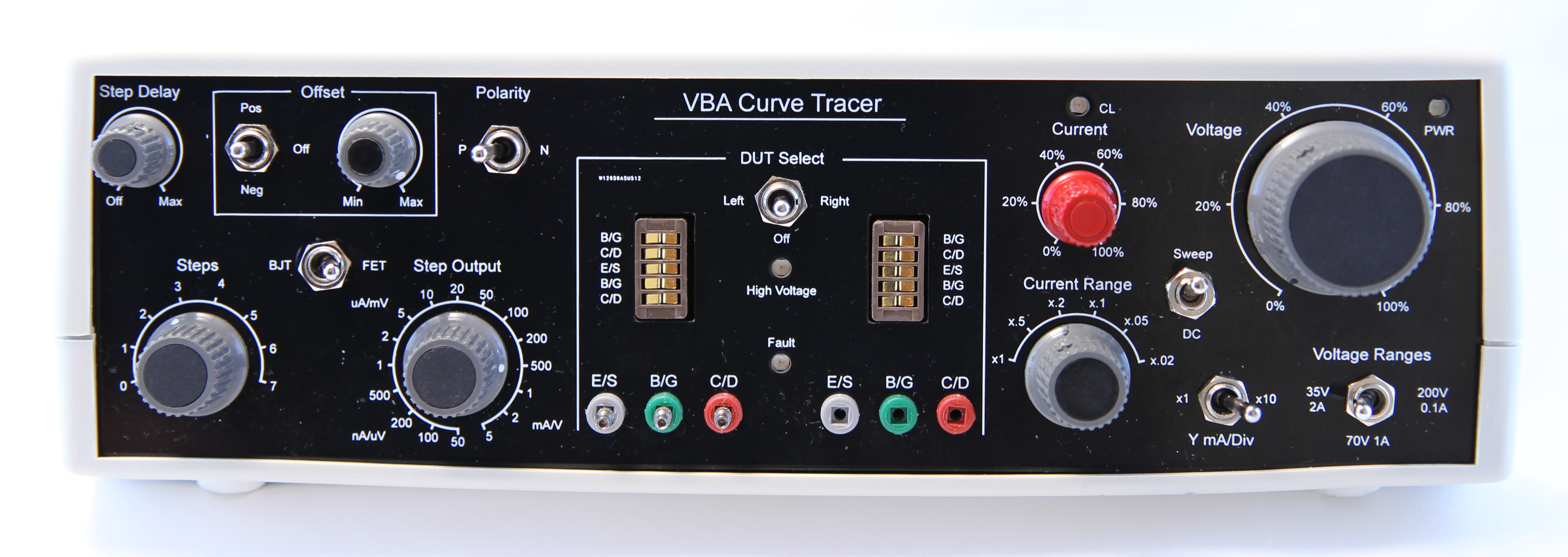
For reference, look at the Face plate above. I'll do the setup going from left to right.
But first, turn the Sweep Voltage to 0% and set the DUT selector to the off position.
It's good practice to do this before every start of a new setup or measurement. It's a good way to prevent DUT losses.
Step Delay should be off. Offset should be off. Select the N Polarity.
Select the BJT mode and select 7 steps. Set the Step Base current output to 50uA/step.
Set the Current Limit to 0% (no output, CL indicator should be on).
Set the current range to x0.05 to create a maximum current of 2A x 0.05 = 100mA.
Set the X-Amp to x10, this is for small signal devices. Higher powered devices will need the x1 setting.
Set the Voltage Range to 35V.
On the DSO, select the X-Y Time base.
Adjust the sampling mode of the DSO to a lower setting, I use 70KPoints to reduce the noise.
Set
CH1 to a Ratio of 10x so the readout is 1:1 with the Sweep Voltage.
Select a limited bandwidth to reduce noise. I use the lowest setting of
my DSO; 20MHz. Set the input to 10V/Div.
Set CH2 to 10mV/Div, 20MHz bandwidth and a Ratio of 0.1x to make the readout 1:1, meaning that 1mV represents 1mA.
To get a feel for what the relationships are in
Volts/Division in relation to the DUT Collector Volts and Amperes we're going to measure, I recommend you to first use a 1K resistor in one of
the DUT sockets between C-E.
Adjust
the vertical positions so the dot is at the cross-hairs of the first
division vertical, and the first division horizontal (the 0V and 0A
origin). This is the I/V origin.
Turn the voltage adjustment so you have a line starting from the origin that will go 3 division to the right.
You should have the following display on your DSO:
CH1, the horizontal Y-channel: We use 10V/Div, with a Ratio of 10x. This will show the Collector voltages at a 1:1 ratio so 3 division horizontally is 30V (VCE).
CH2, the vertical X-channel: We use 10mV/Div, with a Ratio of 0.1x (the ratio of 0.01X you see on the right hand side menu is incorrect) , which results in a display of 10mV/Div representing 10mA/Div. of Collector current (IC).
We use a 1K resistor, and applied 30V across it, resulting in 30mA Collector current. This is represented by 3 divisions vertical deflection of 10mV/Div, or 30mV and that equates to 30mA Collector current.
In case your DSO does not support the Ratio factor, you need to memorize what it shows and always work out the conversion for the Collector current.
Reduce the Voltage and Current adjustments to 0% and remove the 1K resistor.
Set CH1 to 2V/div and CH2 to 20mV/Div.
Plug a 2N3904 transistor in the right DUT socket.
Select the right DUT position to apply power
to the transistor. Turn up the Current to 100%, the CL indicator should be off. Turn up the Sweep Voltage to have 5 divisions
horizontally, which will be a Collector voltage of 10V.
You should now have the following display or close to it:
So what do we see here, apart from the wrong ratio (0.01X should be 0.1X)?
The first step of the cycle is with a Base current (IB) at 50uA, the second at 100uA, the third at 150uA, and so on. We see that the first step shows about 10mV. The 10mV represents a Collector current (IC) of 10mA so the hFE or beta (IC/IB) will be about 10mA/50uA or 200. You could do this calculation for every step or at every IB.
We can see that the beta at the others steps does not change much with higher Base currents and also with different VCE's at
these higher IB's. The gradual changing of the flat lines into a slope is caused by the Early Effect (
https://en.wikipedia.org/wiki/Early_effect).
So what happens when we lower the Base current?
When we lower the Base current to 10uA/Step, and set the V/Div to 2mV, we get the following result:
Note
that the distribution per step is now much a bit more uniform and the lines
stay more horizontal. This is a much better operating area for
this transistor.
We can go even lower, to 1uA/step:

With the current setup, with the Face plate/Front board sandwich and the long wires to make it all work, together with the DSO at 100uV/Div, we have quite a bit of noise.
When we raise the Base current to 200uA/step, we are bumping into the maximum Collector current area of 100mA. Note that the Collector current is now cut-off at about 80mV or 80mA.
Luckily,
we set the maximum current to a limit of 100mA, because without it, we
could have killed the transistor due to thermal stress. If you use your
fingers on the device, you will notice that it will get warm, but with
this current limitation, there is no harm done to it.
We
can measure the device with a higher current limit, but in order to
reduce the thermal stress, we need to activate the Step Cycle Delay
function, and set that to about the maximum. You can probably adjust the delay to a point where the display does not flash anymore.
Now we can select a
higher current range by changing the range from 0.5x to 0.1x, which at a
maximum current of 2A will now be 200mA which is the limit of the
2N3904.
The
transistor is conducting a maximum Collector current of about 130mA and could easily go beyond, but it is Current Limited,
and therefore does not get overly hot. The display does not drift upwards due to
the thermal stress that increases the beta, which is a sure sign that
the device is getting into a thermal run-away that could lead to its
quick heat-stroke death.
Measuring the maximum Collector voltage
This
is not the "official" method but shows a quick-and-dirty way. The
2N3904 is specified with a maximum VCE0 of 40V, lets see what happens
when we raise the voltage. We set the Base current back to 10uA/Step, set the Voltage to 0% and switch to the 75V range. Select the X0.5 Current range and set the Current to 70%. Slowly raise the Sweep voltage to about 55V.
Beyond
40V, the transistor is getting near the breakdown voltage (VCBEO) and
the Collector current begins to skyrocket due to the avalanche effect. This is a
measurement you should make very carefully. The VCBEO specification for this
transistor of 40V is met.
Note
Because
the Collector current goes up fast due to the avalanche effect (breakdown and potentially even punch through), setting
the proper current range and setting the current limiter is very
important because the device can easily get damaged or even destroyed
before you know it.
Below is a properly protected device using the Step delay and current limiting.

Profiling a diode
I'm
using the well known 1N4148 diode as an example. The diode gets
connected between the E and C connections in the ZIF socket. Connect the
Anode to C and the cathode to E. We set the current range to x.05 and
the CL at 25%. Start with the 35V range for the forward voltage. Set the
Sweep voltage to 0%.
Set the DSO hor. channel to 200mV/Div and the vert. channel to 1mV/div.
Set the polarity to N.
Slowly turn up the sweep voltage until current starts to flow.
The voltage when the device starts to conduct can be seen here and is at about 500mV and goes up to about 750mV
with a higher current. The diode has specifications for different
forward voltages at various currents. The specification says between
0.62V and 0.72V at 5mA. That is what we see here as well.
Reduce
the sweep voltage and select the 200V range. Set the hor. channel on
the DSO to 50V/Div Change the polarity to P to reverse the voltage to
the diode. Slowly turn up the sweep voltage until there is current
flowing again, signalling the maximum reverse voltage.
The reverse voltage is about 180V, the specification says 100V. Check!
Profiling a Zener diode
I'm
using a generic 10V 1/4W Zener diode. Set the voltage range back to 35V, and
set the hor. DSO channel to 200mV/Div. Select the N polarity and connect
the Zener diode with the Anode to C and the Cathode to E. Set the
current range to x.05 and the CL at 25%. Set the sweep voltage to 0%.
Select the DUT socket and slowly turn up the sweep voltage until current starts to flow.
The forward voltage is about 680mV at 6mA.
Reduce the sweep voltage and switch the polarity to P to reverse the voltage.
Slowly increase the sweep voltage until current starts to flow.
The Zener voltage, or reverse voltage is exactly 10V at 1mA but increases slightly to 10.1V at 7mA.
Further measurements can be made by increasing the current and see what the Zener voltage does.
Set the vert. channel to 20mV/div. and slowly increase the current by adjusting the CL.
At 100mA, the Zener voltage is now at least 10.2V, something to keep in mind when you design circuits.
Profiling a Schottky diode
I'm using the popular 1N5819 Schottky diode.
As to be expected with a Schottky diode, the forward voltage is about 350mV at 40mA.
The reverse voltage is limited to about 54V.
Profiling LED's
I'm
using a selection of 3mm LED's with different colors to see what the
difference in forward voltages is for the different colors, and also
what the brightness levels are with the same current.
This is a white LED, the forward voltage is 3.4V at 40mA and it is by far the brightest of all.
This is a red LED and the forward voltage is 2.2V at 40mA, and it is very bright.
This is a blue LED with a forward voltage of 3.4V at 40mA, it is very bright.
This
is a green LED with a forward voltage of 2.2V at 40mA, it is the least
bright of all. Note that this has a small amount of forward voltage
change per current, which is why the green, red and also the yellow
LED's can be used in simple constant current circuits.
This is a yellow LED with a forward voltage of 2.3V at 40mA, it is also very bright.
Testing a capacitor for leakage
This is a new test after we added the DC mode for the supply.
In the following test I'm using two 1,000uF/100V 85 degrees C capacitors in series at allow the testing at 200V. These capacitors were actually used in my first prototype, and are probably not of the best quality. The manufacturer is REC.
At about 150V, the leakage current starts to go up and reaches about 4.2mA at 180V.
I also tested a 1uF/450V film capacitor. It showed the following results.
No vertical deflection, so no leakage. We do not show a "dot" because there is some noise on the signal.
2. Device Testing Techniques on a Tektronix CT as a reference
I'm using a number of measurements described in the Tektronix 577 Device Testing Techniques Handbook, available here:
I'm using this information as my guideline, just to see if and how we can do the same tests with our CT.
Testing a BJT transistor
Test 1: Measuring the Collector-Emitter breakdown voltage V(BR)CEO
This is actually the preferred method to measure the C-E breakdown voltage as it is referenced in the textbooks.
The
Emitter and Collector are in the DUT socket while the Base is left
floating (not connected or open - this is the O in CEO). The Sweep Voltage can be in the 75V or 200V range, with the
current range at x0.02 and the CL adjustment at 30%. The X-amp is set at
X10 to have more sensitivity, and the DSO vert. channel is set to a
0.1 multiplier ratio to keep the readout in mV compatible to the IC
current in mA. Start with a minimal Sweep voltage. Select the DUT and
slowly raise the Sweep voltage until the current shoots-up rapidly and the voltage no longer increases. You
can raise the CL limit a bit if it turns on to get a better picture.
In this case, the breakdown VCEO is at about 60V, while the specification is for 40V. Note that the current is about 80mA.
One side effect from this breakdown event is that it also trips the Step protection causing the Fault indicator to come on, even though the Base of the devices is not even connected. This is caused by the violent breakdown event that turns on the sensitive protection circuit which removes the Collector output for about 16mS, after which it is released again. This is an extra protection for the DUT as well because it limits the dissipation and the amount of current.
Test 2: Measuring the Emitter-Base reverse breakdown voltage (V(BR)EBO
In
this test, we will connect the Base of the transistor to the Emitter
socket (grounded Base) and connect the Emitter of the transistor to the
Collector socket. Leave the Collector lead of the transistor floating (not connected).
Set the voltage range to 35V and set the current range to x.02, set the CL adjustment to 40% and the Sweep voltage to minimum.
Slowly increase the Sweep voltage until the current shoots up which shows the breakdown voltage.
The V(BR)EBO is at about 7.8V, while the specifications is listed at 6.0V so the device passes this test.
Test 3 : Collector Cutoff Current ICEV or ICEX
Collector cutoff current is the IC that still flows when the
specified VC and a specified reverse bias is applied. It is normally
less than either ICEO or ICER (collector current with the base open, or
with the base resistively connected to the emitter). This is because
the reverse bias removes most thermal and avalanche carriers from the
base.
Because of non-linearities and the effect of base drive
source impedance, base drive is often specified as a current instead of a
voltage. The symbol ICEX is commonly used for the current method,
while ICEV is used for the voltage method. The current and
voltage drive capabilities of the curve tracer permit either method to
be used.
According to the data sheet for the 2N3904, the specification for ICEX is a maximum of 50nA at a VCE of 30VDC and a VBE of 3VDC.
We can set the measurement up as follows:
Set the voltage range to 35V, and initially set the Voltage adjustment to 0%.
Set the Sweep/DC selection to output DC, Set the Current range to X.1 and the Current adjustment to 40% (about 80mA).
Set the BJT/FET selection to BJT. Set the Step Output to 10uA/Step. Set the number of steps to zero.
Set the offset to Positive and the adjustment to minimum.
Set CH1 of the DSO to 5V/Div, and CH2 to 50uV/Div. The X-Amp should be set to X10 and the CH2 Ratio should be 0.1 for that setting.
Select the DUT and slowly turn up the offset to move the dot to the first graticule line, indicating 50uA.
Increase the Voltage adjustment until you have reached 30VDC.
The reading of CH2 should be no more than 50nA.
Test 4 : Collector-Base Breakdown Voltage V(BR)CBO
With
this test we measure the point when excessive current begins to flow
between the Collector and the Base with the Emitter terminal open. The
Collector of the transistor is connected to the Collector connection on
the ZIF socket, The Emitter is not connected and the Base of the
transistor is connected to the Emitter socket of the ZIF (grounded
Base). The Sweep voltage range is 200V and the current range x0.2. CL
at 80% and the Sweep voltage at minimum.
Slowly increase the sweep voltage until a Collector current starts to flow. You can adjust the CL to a better display.
The V(BR)CBO is measured at 90V, while the specification is at 60V.
Test 5 : DC Forward Current-Gain (DC Beta or hFE)
The DC forward gain is the ratio of the DC Collector current to the DC Base current.
We
cannot really follow the measurement as described in the handbook
because don't have an offset multiplier function. We have an offset, but it
is not calibrated and cannot function as a step setting multiplier. The
reason is that I decided against using a 10-turn potmeter with a scale
for the offset. Adding an offset multiplier function would add more
complexity to the circuit, too much to the price, and take up too much
room on the Front Panel.
We can still do the
measurements, but we will have to use a slightly different approach.
For the 2N3904, the hFE or DC Current Gain with a VCE of 1V is:
- IC = 0.1 mA, hFE is 40 min.
- IC = 1.0 mA, hFE is 70 min.
- IC = 10 mA, hFE is 100 min. 300 max.
- IC = 50 mA, hFE is 60 min.
- IC = 100 mA, hFE is 30 min.
You would normally only do one measurement that is close to the intended application, and I will do the hFE for and IC of 0.1mA.
Set the CT Voltage range to 35V, Sweep. Set the Current range to x.05 and the Current adjust to 80%.
Select 0 steps. Select the Positive Offset and the adjustment to Minimum.
Select the Step output relative to the IC specification. For an IC of 0.1mA and an expected hFE of 40, select 0.1mA/40 is 2.5uA, so select 2uA/Step to get close.
On the DSO, set CH1 to 200mV/Div and CH2 to about 1/6th of the selected IC of 0.1mA. In this case 20uV/Div. which represents 20uA/Div.
Adjust the Voltage very carefully so you have close to 1V on the DSO.
Adjust the Offset so the bottom line crosses the 5th graticule, meaning an IC current of 5 x 20uA or 100uA/0.1mA.
Now we need to measure and calculate the offset factor, because we do not have a calibrated one.
Use a DMM connected between the B-E DUT terminals. Note the voltage that we just set. In my case it was 0.593V. Now turn the offset adjustment to full scale and measure the offset again. In my case I measured 0.675V. To calculate the factor, divide the maximum voltage by the adjusted value (0.675/0.593 = 1.138)
To calculate the DC forward current gain hFE: 5 x 20uA / 1.138 x 2uA = 100uA / 2.276uA = 43.9
Test 6 : Collector-Emitter Saturation Voltage VCE(SAT)
The
VCE saturation voltage is the value of the Collector voltage below
which an increase in specified Base current cannot cause an increase in
Collector current anymore.
The VCE(SAT) is specified at 200mV with an IC of 10mA and an IB of 1mA.
It is also specified as 300mV with an IC of 50mA and an IB of 5mA.
We
set the number of steps to zero, 1mA/step, 35V range, Volt at 0%, current range x0.1, Current at 80%.
Step Delay on and at maximum to protect the transistor from
over-heating. Offset positive and initially at minimum. Sweep voltage at 2.5-3V. On the DSO, set CH1 to 200mV/Div, and CH2 to 5mV/div. ( 5mA)
The following display should be the beginning situation:
Slowly increase the offset until the horizontal line, the IC current level, crosses the second graticule, representing 10mA.
The point where the vertical line transfers into a horizontal line is the VBE(sat) point. This
is the point where no further increase of the Base offset voltage will
increase the Collector current. The VCE(sat) is at about 250mV while the
specification is for 200mV.
Now do the same measurement with an IC of 50mA and an IB of 5mA.
Set the Step Output to 5mA/Step, Set CH2 to 10mV/Div (10mA), and adjust the offset such that the horizontal line crosses the 5th graticule representing an IC of 50mA.
The point where the vertical line transfers into a horizontal line is the VBE(sat) point. Here at about 250-300mV.
This
concludes all the measurements out of the handbook for a Bipolar
Transistor.
More measurements for other devices may be added later.
3. Testing transistor breakdown parameters
Apart from the measurements we just saw earlier, described in the Tektronix handbook, there are a lot more we can make to profile a BJT.
I'm going to follow a list of measurements as they are described in the ON semi AN1628/D Application note for high power BJT's. The same principles apply to small signal ones, like the 2N3904.
A link to the app note is listed above.
The nice thing about this App Note is that they included a little schematic of how the DUT is wired for the various measurements and tests.
I'm going to follow their measurement order starting on page 12.
Breakdown Voltages
BV stand for Breakdown Voltage. This is also shown as V(BR)CEO in some data sheets.
Set the output selector to Tri for Triangle Sweep Voltage waveforms.
BVCEO
This measurement is for reverse Collector to Emitter voltage, with the Base open, under a given Collector current bias.
We already did this measurement above, but here it is again, just for completeness.
Connect the 2N3904 to the DUT socket with only the C to C and E to E leads connected, leave the Base lead open, so flopping in the breeze.
Set the voltage range to 75V, the current range to 0.02 and the CL to 90%, to allow a minimum collector current. Set the Sweep voltage to minimum.
Set CH1 to 10V/Div and CH2 of the DSO to 200uV/Div.
Power the DUT and slowly increase the Sweep Voltage until current starts to flow.
The 2N3904 shows this to happen at 60V, the specification is for 40V.
NOTE
What
can happen when you make this measurement is a case of a snap-back
breakdown,
which is common in this configuration. The Base is open and the
avalanche current (also called first breakdown) is reaching a critical
Base current to cause the
device to enter a second breakdown at a lower voltage. The voltage at
the Base will depend on the level of current limiting and the amount of
resistance from Emitter to GND. I have measured up to 50V on the
floating Base lead with a DMM myself.
This effect is described in the App Note on page 4, Second Breakdown.
We also found that the breakdown or even the punch-through event can turn on the Fault indicator LED because the protection
circuits for the Step Gen are activated as a result of severe glitches generated by the DUT. This event will cause glitches on the Step Gen supply rails and that trips the Fault circuitry and in turn switches the Collector voltage off for a about 16 Milli-seconds and then release it again. The fact that the protection circuit fires does not change the Breakdown Voltage measurement, but it does protect the DUT from harm.
BVCBO
This is the reverse Collector to Base voltage, with the Emitter open, under a given Collector current bias.
Connect
the 2N3904 to the DUT socket with the Collector to C and the Base to the E contact,
leave the Emitter lead open, so flopping in the breeze.
Set
the voltage range to 75V, the current range to 0.02 and the CL to 10%,
to allow a minimum collector current but without limiting. Set the Sweep voltage to minimum.
Set CH1 to 20V/Div and CH2 of the DSO to 200mV/Div.
Power the DUT and slowly increase the Sweep Voltage until current starts to flow.
The 2N3904 shows this to happen at 140V, the specification is for 60V.
BVCER
Reverse Collector to Emitter voltage, the Base connected to the Emitter with a low Ohm resistor, under a given Collector current bias.
Connect
the 2N3904 to the DUT socket with the Collector to C, the Base with 100 Ohm to E and the Emitter to E. Keep the resistor very close to the 2N3904 and use short leads.
Set
the voltage range to 200V, the current range to 0.02 and the CL to 10%,
to allow a minimum collector current but without limiting. Set the Sweep voltage to minimum.
Set CH1 to 20 or 50V/Div and CH2 of the DSO to 200uV/Div.
Power the DUT and slowly increase the Sweep Voltage until current starts to flow.
The 2N3904 shows this to happen at 125V, there is no specification in the data sheet.
The current is limited at 400uA.
BVCES
Reverse Collector to Emitter voltage, the Base shorted to the Emitter, under a given Collector current bias.
Connect
the 2N3904 to the DUT socket with the Collector to C, the Base and the Emitter to E.
Set
the voltage range to 200V, the current range to 0.02 and the CL to 10%,
to allow a minimum collector current but without limiting. Set the Sweep voltage to minimum.
Set CH1 to 20V/Div and CH2 of the DSO to 200uV/Div.
Power the DUT and slowly increase the Sweep Voltage until current starts to flow.
The 2N3904 shows this to happen at 140V, there is no specification in the datasheet.
BVCEX
Reverse Collector to Emitter voltage, with a reverse Base to Emitter bias, under a given Collector current bias.
We do not have a calibrated offset voltage so this measurement could be made, but with an external supply.
Connect
the 2N3904 to the DUT socket with the Collector to C, the Base to a
negative variable DC supply, the positive supply connector to the Emitter and
the Emitter to E.
BVCEY
Reverse Collector to Emitter voltage, with a forward Base to Emitter bias, under a given Collector current bias.
We do not have a calibrated offset voltage so this measurement could be made, but with an external supply.
Connect
the 2N3904 to the DUT socket with the Collector to C, the Base to a
positive variable DC supply, the negative supply connector to the Emitter and
the Emitter to E.
BVEBO
Reverse Emitter to Base voltage, with the Collector open, under a given Emitter current bias.
Connect
the 2N3904 to the DUT socket with the Emitter to C, the Base to E and the Collector open.
Set
the voltage range to 35V, the current range to 0.02 and the CL to 90%,
to allow a minimum collector current but without limiting. Set the Sweep voltage to minimum.
Set CH1 to 2V/Div and CH2 of the DSO to 500uV/Div.
Power the DUT and slowly increase the Sweep Voltage until current starts to flow.
The 2N3904 shows this to happen at 8.2V, the specification is 6V.
Leakage Currents
These measurements are the domain of the DC Voltage. Set the voltage selector to DC.
Note that with our CT, and many others, the leakage current measurements are made in the Collector connection to the positive supply, not in the Emitter connection to the negative supply. In the DC mode, you only see a "dot" representing the voltage on the DSO.
ICEO
Collector to Emitter current under reverse Collector to Emitter voltage, Base open.
Connect
the 2N3904 to the DUT socket with the Collector to C, the Base open and the Emitter to E.
Set
the voltage range to 200V, the current range to 0.02 and the CL to 10%,
to allow a minimum collector current but without limiting. Set the Sweep voltage to minimum.
Set CH1 to 20V/Div and CH2 of the DSO to 1mV/Div.
Power the DUT and slowly increase the DC Voltage until current starts to flow.
The 2N3904 shows this to happen at 82V, when the "dot" changes to a vertical line. The vertical line means that the current is fluctuating wildly. There is no specification for this test in the data sheet.
The amount of current here is about 3.3mA but can be further increased by carefully increasing the CL adjustment.
NOTE
What
can happen when you make this measurement is a case of a snap-back breakdown,
which is common in this configuration. The Base is open and the avalanche current (also called first breakdown) is reaching a critical Base current to cause the
device to enter a second breakdown at a lower voltage. The voltage at
the Base will depend on the level of current limiting and the amount of
resistance from Emitter to GND. I have measured up to 50V on the floating Base lead with a DMM myself.
This effect is described in the App Note on page 4, Second Breakdown.
We also found that the breakdown or even the punch-through event can
turn on the Fault indicator LED because the protection
circuits for the Step Gen are activated as a result of severe glitches
generated by the DUT. This event will cause glitches on the Step Gen
supply rails and that trips the Fault circuitry and in turn switches
the Collector voltage off for a few Milli-seconds and then release it
again. The measured voltage is still indicating the maximum.
Due to the Fault circuit tripping, you will see something like this on the DSO:
There is no "dot" representing the DC voltage, because it switches between zero and the set voltage.
ICBO
Collector to Base current under reverse Collector to Base voltage, Emitter open
Connect
the 2N3904 to the DUT socket with the Collector to C, the Base to E and the Emitter open.
Set
the voltage range to 200V, the current range to 0.05 and the CL to 10%,
to allow a minimum collector current but without limiting. Set the Sweep voltage to minimum.
Set CH1 to 50V/Div and CH2 of the DSO to 1mV/Div.
Power the DUT and slowly increase the DC Voltage until current starts to flow and the dot goes up. If the limiting stops the voltage from going up, increase it a little.
The 2N3904 shows this to happen at 150V. The current is limited by the CL at 2mA, but can now be further increased. There is no specification in the data sheet.
ICER
Collector to Emitter current under reverse Collector to Emitter voltage, Base connected to Emitter by a low Ohm resistor.
Connect
the 2N3904 to the DUT socket with the Collector to C, the Base with 100 Ohm to E and the Emitter to E.
Set
the voltage range to 200V, the current range to 0.05 and the CL to 10%,
to allow a minimum collector current but without limiting. Set the Sweep voltage to minimum.
Set CH1 to50V/Div and CH2 of the DSO to 1mV/Div.
Power the DUT and slowly increase the Sweep Voltage until current starts to flow. If the limiting stops the voltage from going up, increase it a little.
The 2N3904 shows this to happen at 125V and at 800uA. The current can now be increased further by the CL. There is no specification in the data sheet.
ICES
Collector to Emitter current under reverse Collector to Emitter voltage, Base shorted to Emitter.
Connect
the 2N3904 to the DUT socket with the Collector to C, the Base and the Emitter to E.
Set
the voltage range to 200V, the current range to 0.05 and the CL to 10%,
to allow a minimum collector current but without limiting. Set the Sweep voltage to minimum.
Set CH1 to 50V/Div and CH2 of the DSO to 1mV/Div.
Power the DUT and slowly increase the Sweep Voltage until current starts to flow. If the limiting stops the voltage from going up, increase it a little.
The 2N3904 shows this to happen at 125V, with 1mA. The current can now be further increased by the CL. There is no specification in the data sheet.
ICEX
Collector to Emitter current under reverse Collector to Emitter voltage with a reverse Base to Emitter bias.
We do not have a calibrated offset voltage so this measurement could be made, but with an external supply.
Connect
the 2N3904 to the DUT socket with the Collector to C, the Base to a negative variable DC supply, the positive connector to the Emitter and the Emitter to E.
ICEY
Collector to Emitter current under reverse Collector to Emitter voltage, with a forward Base to Emitter bias.
We do not have a calibrated offset voltage so this measurement could be made, but with an external supply.
Connect
the 2N3904 to the DUT socket with the Collector to C, the Base to a positive variable DC supply, the negative connector to the Emitter and the
Emitter to E.
IEBO
Emitter to Base current under reverse Emitter to Base voltage, Collector open.
Connect
the 2N3904 to the DUT socket with the Collector open, the Base to E and the Emitter to C.
Set
the voltage range to 35V, the current range to 0.02 and the CL to 90%,
to allow a minimum collector current but without limiting. Set the DC voltage to minimum.
Set CH1 to 2V/Div and CH2 of the DSO to 500uV/Div.
Power the DUT and slowly increase the DC Voltage until current starts to flow.
The 2N3904 shows this to happen at 8.3V. I then increased the CL until there was no more limiting and the dot did no go up any further signalling the maximum leakage current. At the same time, I increased the V/Div to 5mV/Div. The maximum leakage current shown is 10mA. There is no specification for this test in the data sheet.
4. Profiling a high power BJT
Testing a high power BJT like the MJL3281A is a little different in a few aspects.
The
MJL3281A is a 260V 15A NPN BJT with an hFE between 45 and 150.
It is
one of the transistors we used in earlier Collector/Drain supply
versions, most notably in the Version 1b.
Because this transistor can dissipate up to 200W, we need to be a little careful.
First of all, I switched the current range to x.5 to allow a maximum current of 1A in the 35V range.
I then started with a Base current of 100uA/step. It produced the following result:
The hFE stays evenly spread with the Collector voltage and Base currents. The gain is 9mA/100u is about 90.
If we go to a higher Base current, like 1mA/step, we get the following result:
The
device is not current limited, but only shows 3 steps? This is because
the Y-output amplifier output is hitting the 24V supply rail.
This
is because I did not change the IC current shunt from the X10 to the X1
setting yet. This is in effect a 10X multiplier and this causes the
input signal to hit the supply rail of 24V.
The X10 multiplier is intended for small signal devices to avoid low V/Div settings of the scope.
You could also reduce the number of steps to avoid that, in this case, we can only allow 2 steps.
With
the X1 setting, you also need to change the Y-channel of the scope to a
ratio of 1X to keep the readout consistent. By also increasing the
Current Limiter, we can get the full 7 steps displayed again:
So how does it behave when we apply the maximum VCE0 of 200V?
I
set the Base current to 100uA/step, turned the CL adjustment to 100%
and set the current limiter to x1, to have the full 100mA in this range
at our disposal. I also used the Step delay to reduce the dissipation.
At
higher Base currents, the Collector current is about to shoot up due to
the avalanche effect and the device is getting close to the breakdown
voltage. The dV/dt effect is more noticeable with this measurement.
Be
careful testing the temperature of the device with your fingers, there
is 200V on the collector pad. Keep fingers on the plastic! However, with
100mA, it should not get very warm. Also, make sure you select the right
current setting and use the current limiter to protect the device.
5. Profiling a small signal MOSFET
I'm
using the LP0701 in the TO-92 package, which is a P-channel MOSFET. It
has a VGS(th) of -1V, a DSS of -16.5V, an RDS(on) of 1.5 Ohm and an
ID(on) of -1.25A. So how do we go about testing that device.
First
of all, the polarity should be P, and this will take care of all the
negative polarities of the specifications. It is also a V(oltage)
device, so select FET as the device type. We'll select 7 steps. The VGS(th) is 1V,
so we'll select 500mV/step to get over the threshold, and a 10V sweep
voltage.
Because
a MOSFET can conduct a large current, even though it is considered a
small signal device, we set the current range to X.1 for a maximum of
200mA and set the CL to 50% so we have a safe maximum of 100mA. We also need to set the Y-amp multiplier to X1 and change the DSO channel multiplier to 1x, not the 0.1x we used for the small signal current devices.
Slowly raise the CL limiter to 100%.
So what do we see?
Not
what we expected, right? We see only two steps and the rest is current
limiting at 200mA. The reason is that with 500mV/step, the device is
conducting a lot more current with the higher steps than you would
expect from a small signal device.
Lower the CL setting first and then switch to a higher current range of X.2 which will be 400mA.
Slowly turn up the current limiter and observe the display. Turn it down quickly to avoid too much heat.
This is more like it, but we till can't see the higher steps because of the large Drain current that is limited at 400mA.
We need to lower the volts per step, so we'll go down in current.
At 200mV/step, things start to look a bit more familiar:
However,
we still only see steps 4, 5, 6 and 7. Why? Because step 4 will be at
4*200mV which is the VGS of 1V, when the device starts to conduct so
that's the first step we'll see. Steps 1-3 are hidden from view.
How
can we look at all the 7 steps? We need to go to an even lower step
voltage so now we select 50mV/step to help keep the current in check.
We
now can use the Step offset feature to put the zero(!) step at the
VGS(th) of 1V. We select the negative offset polarity (P-FET) and
carefully adjust the offset to display all 7 steps.
You
may have to raise the current limit to show all 7 steps without
limiting, but turn it down again when you have seen this to keep the
device from over-heating.
The
zero step is now positioned at a voltage of about 1V, so the steps will
further open up the device a step-at-a-time. The beta is increasing
with the Drain voltage, something to be aware of. Note that the Drain
current is almost at 250mA with step 7. You can use your fingers to keep
an eye on the temperature of the device.
To
keep the device from over-heating, we can use the step cycle delay
function that greatly helps to limit the dissipation. Turn it on, and
set it to the maximum. Watch the display and keep your fingers on the
device to "feel" the difference.
Let's
now see what the Breakdown Voltage (BVDSS) is. This is the voltage at
which the reverse-biased body-drift diode breaks down and significant
current starts to flow between the Source and Drain by the avalanche
multiplication process. Turn up the Drain voltage until the device
starts to show this process.
At
about 20V, you can see that the Drain current is rapidly increasing due
to the avalanche effect and is approaching the breakdown voltage. The
specification of 16.5V is easily met. The fact that you see oscillation
can be part of this particular measurement. The device is getting more
and more unstable.
At
this voltage level and because the FET is fully conducting, the device
will get very hot, so be quick, and be careful. Because of the RDS(on)
of only 1.5 Ohm, even the step cycle delay feature will not reduce the
thermal heat enough for a long measurement when you use all steps. Make
sure you use the right current range and use the current limiter to
protect the device from damage or destruction.
A
more prudent method for determining the VDss Breakdown Voltage is to
use only one step, and use the offset feature to just turn the device
on, and then increase the Drain voltage to keep dissipation under
control.
6. Profiling a high power MOSFET
One
of the power devices I used was out of the small selection of suitable
N-MOSFET's we picked for the Collector/Drain supply, the STW6N90K5, a
900V 6A device that has a Vgs(th) of 4V and a Ciss of 432pF.
Select the FET device type.
To
get a handle on the Gate voltage, you really need to use the offset
feature that allows you to set the proper Base step voltage to turn the
device on.
Here is a screenshot taken
with 100mV/Step, 7 steps, 10V and a bit of positive offset to make the
zero step already conduct the device.
The device is getting a tiny bit warm.
To
test it with a higher voltage, and keep the dissipation in check, I
reduced the number of steps to 4. I used the 75V range with the maximum
voltage.
You
can see that the gain no longer climbs up after the voltage is at about
40V, this is a much better operating area for this device. Notice the
beginning of blossoming of the higher step traces due to the increase in
heat.
In the 200V range with maximum voltage, this is the result.
There
is current limiting in effect due to the dissipation that I wanted to
keep in check, even with a mere 100mA. The device gets hot and the
curves start to drift up.
To counter that, you can use the step cycle delay function.
Even
with the step cycle delay activated at the maximum delay, the curves
still drift upwards, a sign that it still gets hot quickly. Note the
beginning of blossoming due to the difference in temperature with the
triangle waveform going up, and then down. This is a very typical effect
caused by thermal heat.
When you need to make longer measurements
with these kind of power devices, it may be wise to add a heat sink to
it and/or use a fan to keep it from a runaway-thermal effect that could
damage or even destroy the device.
With a specification of
900V for the VDSS, we cannot do the Breakdown Voltage test with the
maximum of 200V that is at our disposal.
7. Depletion Mode MOSFET's or J-FET's
JFET's are a special breed in the MOSFET family. In the reference documents at the very top of the page, you can see the difference between depletion mode FET's and enhancement mode FET's. Here is a quick overview from the document I listed.
"Unlike enhancement-mode transistors, which are “normally-off” devices, depletion mode MOSFETs are “normally-on”. N-channel devices are built with P-type silicon
substrates, and P-channel versions are built on N-type substrates. In both cases they
include a thin gate oxide situated between the source and drain regions. A conductive
channel is deliberately formed beneath the gate oxide layer and between the source and
drain by using ion-implantation. By implanting the correct ion polarity in the channel region
during manufacture determines the polarity of the threshold voltage (i.e. -VTH for an N-channel transistor, or +VTH for an P-channel transistor). The actual concentration of ions in
the substrate-to-channel region is used to adjust the threshold voltage (VTH) to the desired
value. Depletion-mode devices are a little more difficult to manufacture and their
characteristics harder to control than enhancement types, which do not require ion implantation."
JFET's are typically used in high quality audio designs, VHF/UHF amplifiers and fast switches, but also have been used in Automatic Gain Control (AGC) circuits for oscillators, to replace the original lamp bulbs. In this case they are used as a variable resistance device. JFET's are a special breed and many of the earlier types are no longer available. Worse, they pre-dated the internet so there is little or no information available anymore. When there even is a datasheet, they are typically lacking in information and sometimes contain no I/V diagrams. On top of that, due to the manufacturing process difficulties, even devices from the same batch have wildly different specifications. (we have been spoiled over the last decades)
There are a few important characteristics that set an JFET apart from other devices, and that poses a challenge based on how we decided to construct our CT. Let me explain. One of the features or characteristics of a JFET is that the device is normally "on", meaning there is the "maximum" current flow (IDSS) from Drain to Source when the Gate is flopping in the breeze or at the same level as the Source. As a matter of fact, when you connect the Gate to the Source, a constant current flows, regardless of the VDS. This is at the so called pinch-off voltage, or VP. That's actually another application for these devices.
The difference in measuring J-FET's
Remember the difference with other devices. For normal N-type devices, we use the Step Generator by increasing the current or voltage with positively going steps towards "fully opening" the device, so going for maximum current. With a N J-FET, the device is already open, so we use the Step Gen steps to gradually "close" the device towards zero current by using negatively going steps to reach VGS=0 where the IDSS current is 0 and there is no current flow.
The pinch-off voltage (Vp)
The Pinch-off voltage is the specific gate-source voltage (VGS) level at which a JFET enters saturation and the channel becomes effectively 'pinched off.' This point marks the transition from the linear region to the saturation region of operation, where the FET maintains a constant current regardless of increases in drain-source voltage. When the gate-source voltage exceeds the pinch-off voltage, the depletion region widens, effectively reducing (pinching) the channel size and limiting the current.
Our VBA Curve Tracer works a little different for JFET's
I made the decision a long time ago to make the operation of our CT as simple as possible, and that meant that the StepGen only produces positive currents and voltages for N-type devices, and negative currents and voltages for P-type devices. However, as we have just seen, N-type JFET's require negatively going steps (-VGS) , which we don't support. (we could but we don't)
Using a traditional CT and the VBA CT
Have a look at the Tektronix document I added at the top of this post for a reference. It explains how you test a JFET for a small signal forward transfer admittance, or the ratio of change in ID to a change between two VGS steps. That ratio is also called the small signal gain.
Because the Tektronix CT's do not have a coupled measurement system as we do, to make it more simple to use for most users, we need to go about it in a slightly different way. The traditional way is to align the 0 step with the IDS trace on the display by vertical movement of the V/Div setting. The IDS trace is the result of the JFET being fully open (by default). You then apply a negatively going second step, and measure the voltage difference (current) between the two curves.
With our CT, we apply the -VGS voltage with the negative offset feature, so there is no more current flowing. IDS=0. We than apply one or more positive going steps (opening up the device, not closing the device) so you can measure the same difference between two curves and arrive at the same conclusion.
However, there may be one more complication.
Our normally recommended offset range is +/-2V, which is sufficient for most applications and many JFET's. However, there are a number of JFET's where the -VGS-off is significantly higher. I have one that needs a VGS of -5V. The J111 can be up to -10V. Luckily, there is a documented modification for the CT that can be made that will change the offset range all the way up to +/-10V. If you are regularly measuring these types of JFET's I suggest you change the offset range for your instrument, and also use the optional multi-turn potmeter for the offset.
My CT currently has the +/- 2V offset range, so I use a "trick" to reach the -VGS-off by using a Lab power supply connected to the 2mm E/S and B/G connectors in the reversed mode, to supply a negative VGS. In addition, you can also use a DMM to measure that voltage so you get an accurate reading of the VGS-off voltage.
2N4391 N-JFET
As an example, I will demonstrate this measurement with the 2N4391 N-JFET from Central Semiconductor Corp. I have two of the older versions, newer ones are only available with the "PBFREE" manufacturing process.
BTW, the versions I have now will cost you $18,25 a piece at DigiKey, and they have no stock for this part at all. Mouser has the PBFREE version for 3,03 Euro's with 2,500 in stock and LCSC has currently no stock but normally sells the PBFREE version for $3,76.
The specification for VGS-off has a wide range in the datasheet, so here is how you measure that.
The JFET is inserted into the test socket. The CT settings are: DUT Select off, Voltage at 0%, 35V range, 0.2x current range, Current Limit (CL) set at 40%, Polarity to N, BJT/FET to the FET position, Offset off, Step Delay off, number of steps to 0, and the Step Output to 500mV/step.
Select the proper DUT socket and slowly turn-up the Drain supply. You will see a curve that looks like the one below:

We see that the device starts to conduct at a VDS of 0V and current moves up in a pretty linear fashion up to about a VDS of 2V and an IDSS of 40mA. This is the Lineair region that is interesting for the variable resistor applications, like an ACG circuit. At about a VDS of 6 volt the device has reached the maximum current of almost 60mA (now in the Saturation region) and that stays pretty flat all the way to the maximum VDS. The transition from the liniar to the saturation region is at the pinch-off (VP) voltage, another other interesting feature that can be used in a constant current application. BTW, the device has a negative temperature effect, so heating up will reduce the current. No possible thermal run-off with JFET's. Note that the device can get pretty hot, so keep an eye on the temperature and keep measurements short.
By setting the number of steps to 0, we actually let the Gate float to it's internally determined voltage.
I measured the VGS to be about 1.21V on one device and 1.88V on the other. This value slowly drops down while the device is heating up due to the IDSS current flow. You can also see that by the curve dropping down a bit.
To measure the zero current point, -VGS-off, we need to apply a negative offset to the Gate. Turn the Offset potmeter to minimum, and select the Neg offset position. Slowly turn the offset from min to max, and you will see the curve flatten downwards. We do not have a calibrated offset voltage measurement, so you can hook-up a DMM between the Source and the Gate. (I use the 2mm sockets for that hook-up)
With my CT, I can only go down to a VGS of -2V, so I can't turn the device fully off, shown by a flat line, so I use my Lab Supply in a reverse hook-up. The positive lead to Source and the negative lead to the Gate. Set the maximum current of the Lab Supply to 70mA (because it needs to sink the current) and start with 0 volts. Turn the supply on, and slowly increase the voltage while looking at the curve until it flattens and there is no IDS current flowing anymore. Note the voltage on the DMM because that is the -VGS-off for that particular device. I measured a VGS of -4.7V on one of my devices, the other one measured -5.1V. De-select the device socket to prevent self heating.
It is allowed to excite the device a little more than the "natural" current, by applying a voltage a little higher than the "natural" VP with a positive VGS. We help that a bit by first lowering the VGS with the offset. Set the Step Output to 500mV/Step. Because the IDSS will go up, you need to select the x.2 current range and set the CL to 40%.
Set the offset to Neg and turn the offset to maximum (I used -2V) and select the device socket. Slowly select a higher number of steps to 4 and you will see the more familiar stepped I/V curves.
BF256B N-JFET
This is a typical JFET used in VHF/UHF amplifier applications.
Nota that this device has a much lower constant current (11mA) compared to the 2N9341.
With the maximum offset of VGS at -2.1, the device almost reaches the VGS-off, it needed -2.8V to fully turn off. I also applied 4steps of 500mV/Step. Note the rumble on the traces due to the sensitivity of the DSO setting at 2mV/Div.
2N5754 N-JFET
This is a JFET for audio and fast switching applications.
It has an even lower constant current of almost 3mA. This device also has a lower VGS-off, so with my CT, I could fully turn it off by applying an offset of -1.5V.
With the input at 500uV/Div, my DSO now shows even more rumble.
Tektronix 151-1021-00 N-JFET
This is a special case and the reason for taking these measurements. This NFET is used in many Tektronix instruments and is no longer available. In the Tek manuals, it is listed as a Siliconix, Inc. FN815. Unfortunately, there is no trace of any documentation I could find. So there is quite a hunt for alternatives going on.
I also use this part in two of my projects, the DIY rebuild of the SG502 a while ago and currently the SG505 oscillator. The SG502 was finished a number of years ago and I have just started a Blog post about the SG505 instrument. This JFET is used in the AGC circuit for the oscillator, a very critical circuit because the very low level of THD is depending on this circuit.
I'm a lucky person to have two devices, saved from the late 70's up until now, with one in my SG502, and one destined to go in my SG505. However, the unobtanium status of this JFET will stop others from building my project as well, so I have started a little search project to find a suitable replacement that is more commonly available, active and for a decent price.
So this is the brand-new, never used 151-1021-00 JFET showing it's mysteries.
The slope is not very steep, and not very linear either. This means that in this particular application, using it as a variable resistor, the VDS voltage must be kept very low. The current is quite substantial at 65mA. It needs a VGS of -5.2V to fully turn it off, quite a lot actually.
So, if you want to use this device in an Automatic Gain Control (AGC) circuit, the slope is important, so I've zoomed in a bit more.
The curve is pretty linear all the way up to about 2VDS, so the lower that voltage is, the better the linearity is. Notice the very slight blooming of the trace with higher currents, an indication of the self-heating due to the current flow.
If we add 3 steps at 500mV/Step with the maximum -2V offset, we will get this:
Note that the blooming is now even more visible due to the higher currents.
If you now look with the same settings again to the 2N4391, it looks very close to the 151-1021-00 part.
I need to do some more tests, but this looks like a decent replacement that is available and still active.
More measurements may be added later...