Building a Curve Tracer - Version 3

Version 3 of the Curve Tracer Project
Based
on the experiences we collected with Version 2, we made some
significant changes to make it a lot more reliable, hopefully easier to
build with commonly available parts, and with greatly increased
usability and safety. In addition, we wanted to see if we can make
more measurements.
More information about this overall project can be found here:
The building of the first version, actually a working prototype with a detailed Theory of Operation.
https://www.paulvdiyblogs.net/2017/
There
is also a description of the second generation based on the first
prototype. This is a fully functional CT that has been built by a few but has some problems and
shortcomings that we're addressing in V3.
https://www.paulvdiyblogs.net/2021/03/building-curve-tracer-v2.html
We now have a fully functional V3 Curve Tracer and we can make measurements. I have started a dedicated Blog with the measurements that we are currently able to make:
https://www.paulvdiyblogs.net/2021/11/making-meassurements-with-v3-curve.html
Note:
We can do many measurements these very versatile instruments can do, but not all. Most likely never will. Not yet anyway. 😏 This instrument is much, much better than some of the tools you can buy online. They are very restricted in their capabilities, something we wanted to address with this design.
Updates on the very latest developments of the VBA Curve Tracer:
June 14 2021
May 31st 2021
Note the date, we finally have a completed instrument! Great!
Here is the unit within the enclosure. The red colored knob is only there because I didn't have a grey one.
May 30st 2021
After solving a few issues, most of them poor solder joints, I'm able to do all measurements and perform stress tests with the maximum voltages and corresponding maximum currents while using an IR camera to look for hot spots. There weren't any to worry about so I put the top cover on and again ran the worse case thermal stress test for about five minutes while pointing the IR camera to the top cover. The camera is so sensitive that you can see the hot spots developing underneath, but the cover itself stays below body temperature. Big sigh of relief!
May27th 2021
First time I was able to put the whole instrument together how it is supposed to fit in the enclosure.


A few items remain to be investigated, tested and resolved, but we're getting really close...
May 24th 2021
I've found the issue with the Step Gen. (below), unfortunately, I still have an issue with the over-voltage protection for one of the Opamps in the Step Gen. I tried, but have not been able to find the problem. With the over-voltage protection disabled, the Step Gen works fine, so I could continue with the verification & calibration, and while doing that, I also updated the documentation as I went. The good news is that everything is working, and I could even do a first initial stress test with high currents. We passed that with flying colors, but this is still without the top cover on and not with the full 2Amps. I need to get my Sandwich wired without the interconnect cable extensions so I can put the cover on. I won't do that yet because I'm still testing and need full access to the boards.
Below is the IR picture of the 35V @ 2A stress test. Nothing gets above 70 degrees C. The hot spots are the current sense resistors and the main bridge. This was to be expected.

While building the instrument, it became clear that we should/could improve on the silkscreen labels to make the interconnections between the boards more consistent, fix some errors and in general make it more clear. We'll also do that on the schematics.
The net-net is that the Main board layout is good, the Face plate layout is good but the silkscreen needs to have a label gaffe on the Face plate fixed. The Front board has a few layout errors that I was able to fix with some cut traces and jumper wires, but we need to go through another board turn to fix the issues and of course update the silkscreen.
We'll wait with the final ordering and publishing until we have sorted out all the pending problems and challenges. We are already in the process of updating the schematics with more or better information and corrections, and also improve the silkscreen of the interconnect labeling of all three boards. When the schematics and Gerber files are published, they will have the latest modifications.
May 22nd 2021
When I checked my e-mails this morning, I read that Mark found out that he made a layout error to the polarity switch, so that needed a fix too. This information confirmed my own observation and saved me some time and the fix was relatively easy to do. Now the X & Y amps are working. After that I tested the Fault circuit and
it seemed to work but no LED. It turns out that these special reverse mounted LED's we use do not have
a reliable cathode indication, and also this LED was flipped, making it
4 out of 4. I ended up using my DMM in the Diode mode to verify the
correct orientation.
Everything seems to be working now but I still have a strange situation with the Step Gen output measured at the DUT connector in the PNP mode. NPN looks better, but is also not quite right. It is related to the over-voltage protection of an Opamp.
May 21st 2021
We fixed the calibration of the 200V maximum issue by eventually deciding to make a calibration resistor value depending on the Volt potmeter tolerance. The circuit was designed for a 100K value, but we found several specimens with only 90K, the minimum of the +/-10% tolerance. The -10% deviation of the potmeter value causes a -20% deviation of the maximum DUT voltage. We will now inform the users of this situation so they can easily calibrate the output to 200V. The other two voltage ranges are heavily influenced by the 200V setting, so this was an important issue to fix.
Having verified the DUT supply side, I switched my attention to the Step Generator circuits and ran into a problem. It turned out that we used a capacitor that should not be there. Removing that fixed the problem I was having. The Step Gen seems to work and a quick check showed that it has the basic functionality. Now on to the X-Y amplifier section where I found that both amps where not working. The X-amp was fixed by correctly mounting a protection diode to the input, because it was reversed. The Y-amp took a bit longer to find. It turned out that Mark made a schematic error that also transpired to the layout. The new offset circuit that we designed was connected to the wrong input pin of the Opamp. Fixing that still did not produce the expected results, but I ran out of time. I suspected the polarity switching and send an e-mail to Mark.
May 18th 2021
I was away from home for a few days and otherwise busy with other chores. I also spend a lot of time writing the instructions that will help users to build the instrument and a list of instructions for Mark to update the schematics and the silkscreens to make it all more logical and self explanatory. I did however complete the wiring between the Main board and the Sandwich. Since then I have been testing the functionality step-by-step. As to be expected, I ran into a few snags on the way, like incorrectly installed parts. It turns out that the special reverse mounted LED's we use on the back of the Face plate have a very poor indication of what the cathode side is. As luck would have it, three out of four were flipped. I can't really blame Mark for getting it wrong because the cathode indication is very difficult to determine. Another issue that I have is that I can't yet get the full maximum voltage of 200V. I thought we fixed that in the 10x10 version, but it's still there. We know we have a tolerance issue with the Volt potmeter resistance, so we need to account for those +/-10% deviations.
May 10th 2021
Apart from a few missing parts that will arrive Thursday, I was able to construct the Sandwich of the Front board and the Face plate and while doing that, also updated the instructions on how to do it. This combination has not seen a power-up yet, that will happen after I installed the missing parts.
Here is a quick-and-dirty picture of where we are now:

May 8th 2021
I managed to build-up the Main board and the Back panel and they are in the enclosure together. All the vital signs I can check on the Main board are there! Very encouraging and a well done job by Mark. I've also written a how-to-build section that includes checking the vital signs while completing the building process. I now need a functioning Front board and Face plate Sandwich to further verify and test the Main board operation and functionality.
May 5th 2021
The shipment from Mark with the new boards in addition to most other parts have arrived so I can start to complete the instrument. It will be slow going because I also want to complete the how-to-build & calibration instructions and need to verify BOM details as well.
April 24th 2021
The latest revision boards have arrived a few days ago and
Mark is busy populating them with the SMD parts. Unfortunately, we are
also hampered a bit by the current chip shortages so we had to make some
changes and order new parts. When Mark has received the last part we're waiting for, he will send the board set and the remaining components to me so I can complete the build and start testing again.
April 8th 2021
The complete set of boards was sent to production. This included a revised Face plate and Front board, the new Main board and the new Back plate. The latest schematics and layouts are added at the end of the Blog. We also started to work on the final BOM's.
March 1st 2021
I got delivery of the two PCB's that Mark designed and
populated. Below you can see how the Front panel and the Front board will
fit together. This also shows how the interface will look
like.
This is just a first test on how everything fits mechanically.
Spoiler alert; it does, with some minor adjustments. We also identified and know how to fix a number of layout errors and silkscreen changes for the next board turn. We're now verifying the operation and also made some changes we want to implement in the next revision.

Here you can still see the major gaffe we made by incorrectly labeling the Vertical channel amplifier gain switch (lower right). It is called X-Amp here, but it should be the Y-Amp. We've had this mistake since the very beginning, just never realized it. In any case, we'll relabel it as "Y mA/Div." to make it more clear that when you flip the gain switch, you also have to change the CH2 input Ratio setting on the scope to keep the 1:1 relationship with the display of the Ic/Id current.
Below is the previous version of the Front board facing the Face plate with all the parts mounted. The two floating potmeters are for the Step Delay and the Offset and are mounted directly on the Face plate (with shorter wires than shown here).

Below is the fully mounted sandwich. The distance between these two boards is adjusted to be 18mm and secured by the toggle and rotary switches and the Current and Volt potmeters that also connect the two ground planes together.

The Main board below is still printed on paper, shown here to give you an idea of how it will all fit inside the enclosure. The green terminal blocks will change to another type in the next revision. The shielded cable connection is there to preserve the fidelity of the Step output signal.

Below is the previous setup with the fully working version of the curve tracer, built with the circuits on 10x10 boards to allow for swapping out new revisions, making measurements and making changes.


The Major Building Blocks
Below is a description of the basic building blocks of this CT. Several of the diagrams and schematics posted here are no longer the very latest version or revision, but serve to describe the functionality. Eventually, that will be the case, and we have published everything on a Github site, but for now, this shows our work in progress.
After this section with the description of our progress and struggles, there is now also a section where we show some of the measurements we can currently make with the CT, and some of the issues.
1. The auxiliary supply

This is the supply for all the voltages for the Op-amps and other parts. There are actually three segments, all fed by one transformer that has dual primary windings for 230V and 115V based main voltages, and equal dual secondary windings. We need dual secondary windings that are isolated from each other because we need a fully isolated supply for the Step Generator.
The black tape in the picture is there to protect me from touching the mains related voltages, because I did not mount the switch that selects 110 or 240V. The dead bug resistor and LED below it is the power indicator, that will be on the front panel. We don't need the large heat sink areas for the regulators and will change the packages of the LM317 and LM337 on the left to smaller ones on the final layout.
One separate winding from the transformer is used for the Triangle Generator, the DUT power supply and the XY amplifier. This supply generates voltages of +10V and -5V. The +10V is used as a reference for a few critical circuits, so this supply is adjustable with a trimmer.

For the final version, we're going to replace the LM337 with a 79L05 regulator because we no longer need a precise -5V due to the way we changed the Triangle Generation.
The Step Gen supply section is the +15V (called plusStep in the schematics) and -15V (minStep) for the Step Generator circuits. This supply is floating (isolated) from all the other supplies and uses a separate winding from the transformer to accomplish this.

The third section is for the X-Y amplifier. It needs -5V (minusXY, the same as minTri) and +24V (plusXY). Because the raw voltage after the voltage multiplier is too high for a 78L24 regulator, we use a transistor and a reference. The 24V is needed because we need a minimum deflection of 20V on the DSO to show the 200V Collector/Drain supply and have enough head-room for the DUT current measurements.

2. Triangle Generator

The left side of this board above is the Digital to Analog (D2A) section, the right hand side the Triangle Waveform Generator. The knobs you see do not belong to these circuits.

3. The AC Power Supply


Adding Voltage and Current ranges
After many deliberations and tests, we decided to offer the following main voltage and current ranges:
- 0-35V @ 0-2A
- 0-70V @ 0-1A
- 0-200V @ 0-100mA.
These voltages are available with the maximum current load. The ranges are created by switching the AC side of the main transformers, and also by limiting the triangle waveform voltage at the input to the Sweep supply. We do this so we can quickly switch from a higher voltage to a lower setting without having a slowly decaying voltage at the DUT. We use MOSFET's that are activated by the Voltage range selection switch to limit the output voltage by reducing the input voltage to the DUT supply. We use resistors and trimmers to ground so we can calibrate each of the three voltage ranges to accommodate for part tolerances.
For each of the three voltage ranges, we also added a current range selection that will allow you to set the maximum current, so you can more easily protect
the DUT. A potmeter on the front panel is used such that you can also set the current in any of these ranges between 0-100% to allow for a further tuning of the current to protect the DUT.
The current range attenuation selections are:
- x1
- x.5
- x.2
- x.1
- x.05
- x.02
This means for example, that when you select the 70V @ 1A range, you can set the current selector to 0-1A, 0-500mA, 0-200mA, 0-100mA, 0-50mA and 0-20mA, and also use the current setting adjustment to go from 0-100% within any of these ranges.
The current ranges are created by a rotary switch located on the front panel that changes the reference voltage for the current limiter circuit. They work in tandem with the already mentioned Voltage range shunts and this is why they have a multiplier and not an exact number.
Part of the Voltage and Current switching is on this AC board, in particular the transformer switching parts. The rest of the circuits is on the DUT Supply Board.
Current Source
There is also a Current Source circuit on this board. It provides a stable 12.5mA load on the DUT power supply irregardless of the voltage, for regulation stability especially when no current flows to a DUT.

With these changes we are currently on Revision 8 for this board.
4. The DUT Power Supply

The DUT power supply is one of the two main sections of the Curve Tracer, the other one is the Step Generator discussed below.
The DUT power supply is made up of two sections. One is the AC supply section supplying the raw DC voltages, and the other one the regulated triangle or DC based buffered output section that we call the DUT power supply.
Initially, we used Opamps to control the Voltage and the Current controllers, and power transistors or Darlington types for the regulation but we were having all sorts of problems to provide a clean triangle waveform at voltages ranging from 0-200V and with currents ranging from open circuit to 2A.
While we were having these issues with the stability, I decided to call in the help from my friend Bud, an ex chip designer from LT. He and I worked together remotely as mouse-pal's on a few other projects, most notably on the UPS power supplies for the Raspberry Pi Model 3 and 4 and a differential scope probe, both described in different Blogs on this site.
Bud's Wild Hair idea.
Bud could not leave the challenges this DUT supply circuit posed out of his head, and started working on a novel and different solution that would accomplish a better transition from voltage regulation into current limiting across the voltage and current spectrum. He called it a "Wild Hair" idea.


The DUT supply Voltage Regulator
The Voltage Regulator

Driving the parallel MOSFET's
Quite novel is the circuit Bud designed to drive the parallel MOSFET's. In most circuits that I know, there is a separate Opamp to drive the second (or more) MOSFET and it must make sure that the load is in effect really shared. That kind of a circuit is a little more difficult to realize in our setup. Good load sharing is not so simple to do in reality, because with the MOSFET's in the linear mode, a minute change in the Gate drive will cause a major change in the conductivity and hence the temperature. Bud came up with a "current duplicator" circuit where he uses an Opamp that measures the current through the main MOSFET, and drives the "slave" MOSFET to conduct the same amount of current. This works really well and I have measured the temperatures to be only about one degree C apart.
We have seen situations by which the amplifier has been blown during a fault situation, so we added diodes to the rails to protect it.The Current Regulator/Limiter


The Current Source & Compensation
Output and thermal stress test

Obviously, the two MOSFET's are the most involved. The picture above shows that the thermal balance between the two is excellent, and I also measured that the temperature of the hot-spot on the device package itself was not above 50C. The three tests passed with flying colors, although this was with everything in free air. We need to do the tests again when everything is inside the enclosure, but it looks like we have the thermals under control with a normally operating CT and don't need a fan. More extreme/fault tests are described below.
DUT protection circuit

High Voltage Warning Indicator
We
wanted to warn the user when dangerous voltages are present on the DUT
output connectors. We determined that this is at about 40V and higher.
Mark came up with a
simple method that just uses a single transistor to drive the LED on
the front panel when the 40V threshold is exceeded. After adding the DC
mode, we needed to make sure the circuit now tripped with both voltages at about the same
level. The negative DC voltage enters through R29 and R30, and is
blocked by C1 to reach the lower value resistors. The triangle voltage
enters though C1, R1 and R2. We use two resistors in series to take care
of the up to 200V, and it also allows a trimming of the tripping
point. The diode clamps the voltage level for the transistor. This circuit is currently on the AC Supply board.

5. The Step Generator
The Step Generator PCB consists of two parts, the Digital to Analog (D2A) circuit with the step generation and second the buffered output amplifier that drives the DUT.
The D2A section


Dealing with thermal issues
When
you're testing devices with higher currents, there are two effects you
have to keep in mind. One is that the self-heating of the device while
you are testing, can distort the I/V display because of an effect called
looping. This is caused by the way the DUT is activated. With the
single step level at the Base, the Collector is getting a raising
voltage due to the triangle based supply. The higher the voltage
becomes, the higher the thermal heat will be. This typically results in a small gain change, so the curve will bend up a little. If the triangle
voltage now goes down during the same step, the heat dissipation gets less and the gain
changes again so the curve will bend down a little. This causes the
typical elliptical looping of the traces. Below is an example of a very
minor case shown on a Tektronix CT.

The thermal heat of the DUT die can increase very rapidly and can get very hot, so much so, that you have to stop the test to let it cool off again. If you don't notice it in time, your DUT may have been damaged or even died of a heat stroke already. With high currents needed for power devices, you can't even run the test for more than a few seconds and the looping of the trace can become so big that it will be impossible to interpret.
There
is a way to cheat however. When you select only one half of the triangle waveform per step, you can
eliminate the looping effect. This is what we do now standard with this version 3. When you use a half sine-wave, as the Tek
576/7 do, that trick is not possible. Look at the first Blog of building
the CT project to see a more elaborate description.
Professional Curve Tracers allow you to use a pulsed step mode, by which there is a pause after each complete step cycle. This gives the DUT some time to cool down before the next step cycle arrives.
I implemented a
similar functionality for our Version 3 by adding a 555 timer and a few components to the
Step Gen circuit. With a potentiometer adjustment, it adds several Milli
seconds of delay between step cycles. The delay is synchronized with
the end of the step cycle, and can be applied for every number of steps from 1..7.
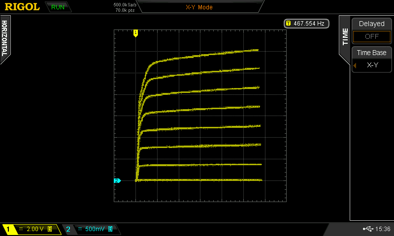
Below are two screen shots that show this feature in operation on a prototype. The first picture shows the normal operation but shown in the time-base mode of the DSO. The yellow trace is the triangle waveform for the collector voltage, and the blue trace is the Step Gen cycle that repeats itself after one 0 to 7 step cycle.
The second picture shows the delayed step function. It starts with about 40mS delay between the full step cycles. This can be extended to about 150-200 mS by using a potentiometer on the front panel. This is the practical maximum because the trace starts to "flicker" due to the pause between the X-axis acquisitions. The display can be adjusted somewhat by changing the time/div. setting of the DSO to make it as smooth as possible. The delay between the cycles allows the DUT to cool off a bit.


The Buffered Step Gen Output Section


The offset circuit in more detail
Pot20 can supply up to ±15V to the offset circuitry by eliminating R21. The polarity is controlled by toggle switch S20. R21 is in the circuit so one can program lower offset voltages without wasting pot travel which also adds granularity. With R21 at 0 ohms it means the offset you can start with is plusStep and minusStep (±15V). The offset coming from Pot20 is buffered by a unity gain buffer U21A. This buffer drives the independent circuitry for the BJT and the FET mode.
BJT offset circuit:
For the BJT offset, U20A adds the offset from the buffer U21A to the
step signal. The offset gets divided by 2 by R31 and R32 and fed to the
non-inverting input of U20A, that has a gain of 2. This means that the overall offset is the voltage fed from U21A.
R21, R31 and R32 determine the total amount of voltage offset you can apply.
FET offset circuit:
For FET type devices, the offset is not added to the step voltage. It is an offset that is
applied directly to the Gate bypassing the step function circuit. This was done because
of the varying VT of most FETs and to set the Vp for JFETS's. This offset allows the FET to be at
VT to make each step sent to the Gate useful or meaningful. The offset is summed
into the Gate drive with the already defined steps at the step voltage selection with values between 50uV and 5V.
The selected voltage steps and the offset are summed by U23A. U23A has a gain
of 2. The steps are divided by 2 before entering the U23A input. This is done by
the combination of R34, R35 and R38. For the Opamp, R34 and R38 are in parallel and form a
voltage divider with R35. R34 and R38 in parallel should be equal to R35 to keep the divide by 2 outcome before entering the positive input of U23A.
When you want to change the offset range from the +/-2V that is pre-selected with the values in the schematic diagram, you need change 3 resistors while retaining the divide by 2 relationship.
This factor defines the requirements for R34, R35 and R38. To make it easier, Mark has created a spreadsheet to help select the resistors needed to give different offset voltages while maintaining the relationship and the divide by 2 factor. This spreadsheet is available on the Github in the Front Board section.
Protecting the Step Generator
In the post about the Version 2 CT experiences, I already described the massacre that happened when there was a major catastrophe with the DUT power supply. This event showed that the Step Gen was not protected from the high voltages that could make their way into the Base/Gate circuit and cause havoc in the Step Gen circuits
Opamps have a really hard time dealing with voltages on the inputs or outputs that are greater than the supply voltages. In our case, they are +/- 15V, while the Collector supply can be as high as 200V.
If you consider that there is only a single N- or P-junction sliver of maybe a few microns separating the Collector from the Base on a DUT die, its easy to imagine that this can go horribly wrong. If you blow the Collector-Base junction, you have a serious problem. When I examined the 2N3904 or 2N3906 transistors that I blew up, there were several that suffered from a damaged C-B junction for the NPN or a damaged E-B junction for the PNP. In those cases, that resulted in a low junction resistance, putting the full Collector voltage through the Base back into the Step Gen output and blowing-up parts.

The output of the Step Gen Buffer circuit, also going to the Base/Gate of the DUT, comes in on the left hand side of the diagram. Diodes D1, D2 and the two opto-coupler diodes work together to create a Fault signal. When the Base/Gate voltage is going beyond one of the +/-15V supply rails, actually at +/-18V, one of the opto-couplers will fire and turn on the dual transistors configured as an SCR. The SCR flips and will turn on both MOSFET's. Q3 will strangle the input to the DUT power supply and completely removes the output voltage. Q4 is used to turn on a Fault indicator on the front panel so the user is alerted.
The R/C set by C1/R9 will release the SCR after about 16mS. When the fault is no longer there normal operation continues otherwise the output remains clamped.
Step Gen Fault Protection Test

The triangle is at 17.6V, just below the tripping point. The CH2 shows the Base voltage.


Extending the Step Gen attenuation ranges
It had always been difficult if not impossible to measure high gain devices like Darlington transistors with the previous versions of the CT. The lowest setting of 1uA/step was still far too high, so we added 4 more settings by switching from a 12 to a 16 position rotary switch. The added settings will be for 500, 200, 100 and 50nA/Step. Unfortunately, the change from a 12-step to an 18-step rotary switch is a costly one. Luckily, the switch is a lot smaller in size which helped tremendously with the layout of the Front board and the Face plate.
6. The X-Y Output Amplifier and DUT circuit

Dealing with the XY display noise level
Because I'm using a relatively inexpensive DSO, a Rigol DS2072A, most of the Y-axis displays for small signal transistor currents are very noisy on my DSO because I have to use V/Div. settings that are in the mV area and they show a lot of noise. It's not so much the DSO itself that is noisy, but the combination of the DSO input circuitry, the way XY plots are made with a DSO and the pick-up of noise that makes the traces very fuzzy.
BTW, if you're interested to learn why DSO's seem to be more noisy than CRT's, there are two nice posts on Youtube that go into the details and can be found here: EEVblog #601 and also here EEVblog #610.
Both Mark and Richard use more professional scopes and they don't have this issue. There are two solutions. We can add another Opamp with higher gain, but that will also amplify the noise from the source. The other solution is to use a higher value shunt. Both solutions will allow you to avoid the lower level Volts/Division settings of the DSO.
I decided to use two different Ic shunt resistors, because using a single 1 Ohm resistor does not make sense. (pun intended)
By adding a toggle switch to the front panel, the user can now select a 1 Ohm and 10 Ohm shunt resistor values, in effect multiplying the IC current by x1 and x10. This will allow you to use V/Div. settings that are a factor ten higher and therefore more devoid of noise and we will have a better sensitivity at lower currents as well.
Here is a measurement taken with the 1 Ohm shunt, and a 2mV/Div. setting on my Rigol.

Here is the same measurement, but now with the 10 Ohm shunt, allowing you to go to a 20mV/Div. setting.

Note that this was made with the "dual triangle sweep" per step. Also, the small "opening" in the trace for the second step is caused by the period the DSO needs to process the acquisition of the collected data. This "hole" only shows when you make a screenshot. Look at the first post of building a CT for more information.
Small offset on the Y-axis
Richard
has found that on his Version 1 CT there is a slight offset of the X-Y picture.
This is probably caused by part tolerances. He fixed it by shifting the
output of the Y-Opamp a little with a high value resistor to a rail. We've added a trimmer circuit that solves the problem by adding a small pos or neg offset calibration to the Opamp.
We have a fully functioning testbed for the Version 3 Curve Tracer

This is a picture with the latest revision 10 x 10 boards with the last modifications, resulting in a design freeze. (yeah, right... I was way too optimistic, several changes were made after we got the "final" boards, and even then...)
Here is what you see on the picture:
The red board top left with the transformer on it is the Auxiliary Supply.
To the right of it is the AC supply with the green color and with the very large main capacitor.
Above that is the main AC supply transformer mounted on the back-panel of the enclosure with the main socket and filter, a mains fuse and mains switch. To the right of the AC supply is the 120VAC transformer used to create the 200V. The plastic back panel will be replaced by a PCB.
On the top right is the red board for the DUT power supply. It has the large heat-sinks on it where the MOSFET's are mounted on. The two potmeters are the Voltage selection and the Current setting. The current ranges are selected by a jumper. The switch you see on the lower corner is a prototype for the DC mode selection.
In the middle you see a blue board that is the Triangle Generator and D2A section with the Step Selection. The number of steps is selected by a wire jumper.
To the lower left in black is the X-Y amplifier board with the DUT section. There are two small coax cables in grey going to my DSO.
The white board in the middle is the Step Gen Buffer output board. The potmeter to the left of it is for the Offset adjustment. Mark had an idea to use a divider jumper to reduce the Step outputs so we could use less expensive rotary switches. With this 10x10, we can use a simple jumper on a row of pins to select the output settings. Unfortunately, Mark's idea did not work in reality, so in order to add the 8 lowest settings, I used a small test board with THT resistors and a 16 position rotary switch instead of the jumper selection to create the full range. It is not pretty, but functionally does the job although, not surprisingly, there is a lot of hum and noise in the lowest uV/nA settings. We will not make another revision for this board but will now go straight to the Main and Front Board design.
First measurements to test the functionality
Below is a measurement of a 2N3904 as an example (20uA/Step) using the single slope triangle method.
First is the traditional Time-Base picture of the Collector voltage and the Base current and below it the I/V plot in the X-Y mode. The Step is not flat because the Collector voltage will change the gain, and hence the current. You can see that with higher steps (current) the flatness changes quite dramatically. This shows up in the X-Y plot with upwards going slopes at higher Base currents (the Early effect). This is quite typical for a 2N3904. There are other transistor types where the lines stay horizontally flat for every step, meaning that the gain or beta performance is more uniform across the Base current or Collector spectrum.
You need a Curve Tracer to see this effect.

Also note how much cleaner this X-Y plot is with the single slope method compared to the Version 1b and also the Version 2.
We identified a few issues that we were able to resolve or fix already and are working on a few things we need to try, possibly involving yet another board turn, but the CT is now fully functional and a lot of testing and profiling still lies ahead of us.
The BJT dV/dt problem
While profiling the CT, we stumbled on a rather strange phenomena that we're trying to understand and see if we can explain it, or better yet, design it into oblivion.
This phenomena shows up at very low Base currents for BJT devices, and also with higher Collector voltages and then also with higher triangle frequencies. For reference, look at the screen shot above made with a 20uA/Step and a 12V Collector voltage. When you reduce the Base current to lower levels, we see a change in the Step function. There is a sudden drop when the Collector voltage (the triangle) changes direction. This drop in the current creates a double line display for every step. Below is the Time-Base picture to show the situation at 1uA/Step. Below that is the X-Y plot with the resulting double lines due to this drop.


I'm pretty certain this is all caused by our current test rig setup.
To continue to test and profile while trying to minimize this effect, I lowered the base frequency to about 155Hz, almost removing the effect. My DSO display is still very nice at this repetition rate so no harm is done, although it may be different on an analog scope. The new 555-based triangle generator has a calibration for the frequency that can now be easily set from about 140 to 650 Hz.
UPDATE
I did the same test as above with the new Front board and Face plate, and the problem is now completely gone with a frequency around about 200Hz. However it still comes back with higher frequencies (at 1uA/35V) so we're not fully out of the woods yet. More will need to be tested when we have the final instrument in the enclosure.


DUT Breakdown/punch-through effect issue

The top trace shows the glitches on the isolated GND of the Step Gen, and are also visible on the +/-15V rails. Note that the CH1 scale is incorrect, it should be 1V/div. (wrong multiplier) The glitches turn on the Fault detection system, shown here in the bottom trace.


We worked together to find the root cause, because we designed the instrument to be normally very stable and it will not show oscillation. During the design phase, we went through a lot to make sure it is inherently stable, so I helped Matt to take a deeper dive. Here are some of the findings from Matt in different configurations.


Notice the hash during the current limiting phase (the flat portion of the triangle), that also shows up on the top portion (highest current) of the I/V curve in the X-Y mode. This is caused by the additional inductance of the leads connecting to the instrument.

So the moral of the story is to keep the length of the DUT leads as short as possible, or shield them.
Stay tuned for more.
If you like what you see, please support me by buying me a coffee: https://www.buymeacoffee.com/M9ouLVXBdw