Before you read on, you should know that after building two versions of the DIY kit, I was not very impressed about the stability, noise, but above all, the complete lack of any form of protection. Think about that before you connect something valuable to the supply.
Subsequently, I designed a more modern power supply that you can follow here: http://www.paulvdiyblogs.net/2017/07/my-new-power-supply.html
After building two of them as well, and learning a lot and have a lot of fun experimenting and building, I still decided to purchase a lab quality professional power supply. That should hopefully tell you a few things. In the mean-time, we're now in 2026, and I decided to build yet another Lab Power Supply, this time based on a Tektronix design, the PS503A. That process can be found here:
https://www.paulvdiyblogs.net/2025/12/diy-ps503a-rebuild-prototype.html
and here:
https://www.paulvdiyblogs.net/2026/03/diy-ps503a-construction.html
There are many things you can learn about the kit in this post, and also select possible improvements, but please understand that I can't really help you anymore. It's been too long ago.

Due to a move, I recently sold my large lab PSU, and needed a substitute. I wanted to be a little more flexible, and did not want a huge and heavy supply on my bench anymore.
Searching the web, I came across an inexpensive DIY kit that implemented a very popular design for a power supply. I seldom if ever need more than 1A, so I used the kit to tune it to my liking, and also added the latest modifications for the original design.
I added an LCD display and one addition to the original design is a current setting mechanism, using the display, so you can set the current limiting or constant current mode before connecting the DUT.
I have built two supplies and can connect them in parallel to get more current, or in series to get a true dual +0..30V *zero* -0..30V supply or a 0..60V supply. One is designed for 3A and one for 1A max.
After some fiddling, I also designed a simple dual tracking system when the two supplies are used in series, so one supply controls the other.
Enjoy!
paulv
Tuning a 0..30V 0..3A PSU kit
So much so, that
several Chinese suppliers have created a kit with just about all parts
including a PCB for a very attractive price. I paid $12.64 and that is with
free shipping. On top of that, it took less than 2 weeks for the kit to arrive.
I purchased something this one:
Note that this link
may no longer work over time, just search for “AC 24V 0..30V 0..3A DIY kit” and
you shall find…
If you buy the parts
from a usual on-line supplier, you probably spend more on the shipping cost
alone. So where’s the catch?
The kit is based on
the original article and has some issues that need to be addressed. There are
several postings on the electronics-lab forum that go into great details about
the original design:
However, if you adhere
to a few simple requirements, you can use this kit without too many changes and
create a fine supply for your bench that will probably be adequate for 90+% of
your power supply needs.
Here is the constraint:
If you stay below a maximum current of 1.5A, the kit will work perfectly with a
couple of changes in the components and we will discuss that here. The kit can
also be extended with more functionality and that is also discussed here.
To start off, several
components supplied with the kit (the list is at the very end of this post) are different from the original design, so
let’s go over those:
D7 and D8 are 1N4733A 5V1
zener diodes, and they require 49mA for a bias. This deviates from the original
design that has low current 5V6 zener diodes with a lower bias. Q3 is a 2SD9015
and Q1 is a 2DS9014. Q2 is a 2SD882 and Q4 is a 2SD1047. Q4 is much easier to
mount on a heat sink, compared to a 2N3055.
Most other parts are following the
original design, however, a few resistors supplied with the kit have a wattage
that is too low. R2 of 82R should be 1W, R3 of 220R should also be 1W. The
supplied 0.25 Watt resistors will get too hot. R1, which is 2K2 1W will also
get pretty hot, so mount that a little above the PCB, or replace it with a
2Watt resistor. R7 should also be mounted a little above the PCB.
An extra part that is
not in the original design is an LM7824, to create a 24V DC supply for a fan.
If you are like me, you will have a lot of 12V fans, because that is the
voltage used in PC’s. In any case, I switched the LM7824 to an LM7812, because
I drive a few additional LED’s with it, and also supply a Volt/Ampere display
with it. If I decide to change the unit for a higher current, I may need a fan,
and I have several 12V DC fans in my stash. If you decide to keep the LM7824,
double the resistor value that go to the LED’s. The meter can handle the 24V.
(see below) You can mount the LM78XX on the PCB, but I didn’t. It gets pretty
warm, so it went on the heat sink.
If you are going to
limit the maximum current to 1 or 1.5 Amp, there is no need to go fancy on the
transformer, and you can use a more or less standard transformer with 24VAC and
1 or 1.5A current.
The supplied TL081 op amps’s have
a deficiency that we will want to avoid, so we will not use them.
The kit comes without
a schematic, parts list or PCB layout, although the stenciling on the PCB shows
the values, but not the part numbers.
Let’s go over the
changes I made to the original design. Here is the original schematic:
The parts list
supplied with the kit is listed at the end of this post, with the changes and additions.
From that supplied
parts list, we will not use D7 and D8 is a 1N4733A 5V1 zener needing a 59mA
bias. We will replace this type with a BZX55C5V6 or BZX79C5V6 zener, both
requiring only 5mA bias current. U1 will set the reference voltage to twice the
zener voltage so 11.2V. With the required 5mA bias for D8, R4 should be 1K, not
4K7.
Because we need to limit the maximum current to either 1 or 1.5A, R18
needs to be recalculated. This resistor had the wrong value (56K) in the
original design anyway.
Here is a simplified
diagram to help with the calculation, just in case you want to use another
maximum current version:
Let’s see where the original calculation for R18
went wrong, and resulted in a maximum current that would literally blow a fuse,
or more.
To calculate R18 for a maximum current of 3A:
Vref = 2 x D8 of 5V6 = 11.2V
Voltage over R7 of 0.47R at 3A is
= R7 * Imax = 1.41V
At max current setting of P2, the
top is 0R and the bottom is 10K
P2+R17 = 10K + 33R = 10033Ohm
For the equivalent circuit:
R18 = P2+R17 * (Vref+VR7 - VR7) /
VR7
Or
R18 = 10033 * (12.61 – 1.41) /
1.41 = 79K694
The original value was 56K, but
that would mean a maximum current of :
VR7 = 56000 / (56000 + 10033) *
12.61 = 1,916V / 0.47R = 4A! Oops…
The following values are
calculated for R18 with the new low current 5V6 zener diode for D8:
R18 = 72.5K @ 3.0A
R18 = 169 K @ 1.5A
R18 = 259 K @ 1.0A
If you want to be
precise, you can still use the original R18 value of 56K, but add a trimmer of
200K or 250K in series. This trimmer can be mounted on P2, so you don’t have to
mess with the PCB.
So what else was wrong
with the original design, (if!) we keep to the 1.5A max. Well, the original
design used Op Amps that had a flaw.
Several more changes
are related to their replacement. Because we will not use the TL072, we can
drop Q1, R13 and R14. They were needed to remove a glitch from the output that
was caused by the TL072. The circuit around Q1 was designed such that as soon
as the negative 5V6 supply collapses, when the mains is switched off, it would
immediately turn Q2 off, and therefore also the output. With Q1 in place, it
would protect the Device Under Test or DUT from voltages higher than what you
set the output to. That can be deadly for the DUT.
Unfortunately, the
circuit around Q2 is still not perfect. There were still situations by which a
glitch was introduced at the output when the main supply is switched-on or
switched-off.
Let me show you:
Switching on: The top
trace (A) is the output of the PSU at 25V and with a 500mA load. The bottom trace
is the negative supply. The negative supply goes down from 0V in the rhythm of
the main frequency, in my case 50Hz, until the D7 zener kicks in. The base of
Q1 is set to 0V by R13 and R14, but this setting is upset with the supply
“swinging” into place, turning Q1 on and off. Depending on the point in time when
you flip the switch in relation to the main frequency, you will see this
behavior. If you try it 10 times, you may see this effect once or twice.
So what happens when
you switch the supply off at the mains level?
Bottom trace is the output to the DUT. So there is another glitch that can happen. Not always, but it can happen.
So, although the
circuit around Q1 did a good job as intended, it removed large spikes above the
output voltage setting, it was not perfect.
By replacing the three
TL072’s with the TLE2141, we can eliminate the Q1 circuit all together. Furthermore,
with the new op amps, the negative supply can be reduced from -5V6 to about
-1.3V. That’s why we will not need D7.
We’re not done with
the negative supply yet. In the Current Limit (CL) mode, for all practical
purposes, the supply actually switches to a Constant Current (CC) mode. U3 does
not switch from rail to rail, but switches to about +3V. This is enough to turn
the CL LED on, but there is still a voltage at the output. You can now slowly
turn P2 counter clockwise, and you’ll see the voltage at the output drop, while
the current stays the same. This is the Constant Current mode. So in the CL/CC
mode, the output from U3 switches from the positive supply of 26V to about +3V
and then slowly goes to the level of the negative supply, at which point the
output at the terminals is removed completely.
Unfortunately, this is not
really a great CC mode, if you look at the voltage output supply:
There are two sources
for the 1.7 V p-p “noise” riding on the output of the supply. One is mains hum, the result of
the rather crude way the negative supply is concocted. The higher frequency
noise is the result of the closed-loop activity between U3, U2 and the output
stage. U3 and U2 are in a constant battle to keep the output high (U2) and at
the same time, U3 is limiting the output to stay within the current limit.
There is little we can do about that without doing a major redesign, but we can at least
remove most of the mains ripple.
We do that by
replacing R3 with an LM337 voltage regulator (U6), and we set the output level
at -1.3V with two additional resistors, R25 and R26. We’ll also add a small
filter capacitor, C14 of about 22uF/10V.
If you have a habit of
supplying your DUT with power by turning the PSU on and off, even with the above changes, you may still introduce
a glitch in the voltage at the output terminals. I have experimented with a few
possible solutions, but gave up because I could not find a simple solution to
fix this.
Here the mains is switched
off while we’re looking at the output voltage. The slope is depending on the
current that is pulled from the supply, so that curve may be steeper, but it’s
still not very pretty.
Here the main power is
applied while the output has been set for 3.3V, the most critical voltage level
for devices under test. Notice the large spike that significantly exceeds the
maximum voltage that has been set.
So to still allow a
clean turn on and turn off to the DUT, I added a double throw switch into the
mix. One part of the switch connects the anode of D9 to ground, because this
will remove the power from the output. To show myself that there is no power on
the output, the other half of the switch turns on a red LED. The LED is
connected between the 12V and via a 4K7 resistor to the switch, which connects
it to ground. Simple and effective.
I also wanted to have
a Voltage and Current display, so I purchased one of these:
These are below $10 on
Amazon or eBay. The small red and black wires on the right provide the power to
the logic of the unit, and that can be anywhere between 3.5 and 30V DC. I
connected them to the LM7812. Note that these displays should really be galvanically seperated from the supply to avoid noise injection. The alternative is to do some serious filtering in the supply voltage chain to avoid that noise.
These displays are
capable of handling a car battery or big motor currents (up to 10A with the
internal shunt), and therefore the current and voltage sensing wires are very
thick. I replaced them with different wiring. In any case, the red wire is
connected to the output of the PSU, and is the voltage sensing input. This
device has an internal shunt resistor, and that is connected between the yellow
and black wire. To make it easy, I connected the black wire to the minus output
of the PSU (4) and that makes the yellow wire the “new” minus output. The shunt
will make a tiny difference because it sits outside of the feedback loop, but
the error is extremely low, because the shunt is extremely low in value as well.
On the back of the
unit are two tiny trim pots you can use to adjust the voltage and current.
There are two more
additions that I made. One is to add an LED to show that the unit has main
power. That green LED is connected between the 12V and through a 4K7 resistor
to ground.
The final addition is
another 3300uF/50V capacitor (C12) parallel to C1, to give more stability to
the raw supply and to reduce ripple at higher currents.
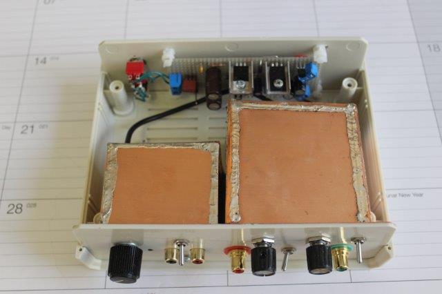
I used a large heat
sink, and mounted the LM7812, Q2 and Q4 on it. There is plenty of room to add
another output transistor parallel to Q4, if I decide to increase the current.
With this heat sink, I
will not need a fan with the current staying below 1.5A.
From left to right: Q4, Q3 and the LM7812.
Q4 and Q3 are
isolated, the LM heatsink is ground, so does not need it.
To create the front
panel, I printed a design on photo paper, used double sided tape to fix it to
the metal front panel and cut out the holes.
Here is where the 24V
AC comes in. I can use different size transformers, and use them for several
applications this way.
I did not use the
supplied 10K pot meter for the current setting, because it did not come with a nut.
It needs an M7 nut I didn’t have, so I used another 10K pot meter I had in my
stash.
After I finished all the modifications and started to experiment with the supply,
I saw the need to add a way to show the current limit setting, so I have now added
a little circuit to the supply so I can set the Constant Current/Current Limit.
Because I already have a voltmeter, the easiest method was to use that to show
the current setting. However, showing the value on the current meter display
with the unit I use is tricky.
To show the current setting on the voltmeter, all we really need is a
convertor that translates the current limit setting to a voltage.
To show the relation of 1A = 1V, with R7 at 0.47R, we need a multiplication
factor of 1/0.47 = 2.127.
By using an additional op amp (U5), we will make this circuit independent of
the maximum current of the PSU.
If you look at the schematic, the circuit around U4 implements that function.
RV2 can be adjusted by setting P2 to the maximum value of the current, say 1A.
You can measure the voltage at the wiper of P2 with a DMM and set P2 to read
1.00V on the DMM. If you implemented R18 in combination with a trimmer, adjust
that trimmer first to show 1.00V with P2 at maximum. Push the CC set button and
adjust RV2 to have the voltmeter of the PSU show 1.00V as well.
Here is the final schematic:
Here is the original
parts list as supplied with the kit, but with my changes and additions listed as
well:
R1 = 2K2 1W Replaced
with a 2W version
R2
= 82R Replaced
with a 2W version
R3
= 220R Not
needed (replaced with an LM337)
R4
= 4K7 Value
changed to 1K
R5,
R6, R13, R20, R21 = 10K R13
not needed
R7 = 0.47R 5W
R8, R11 = 27K
R9, R19 = 2K2
R10 = 270K Value
changed to 1K
R12, R18 = 56K R18
see text
R14 = 1K5 Not
needed
R15, R16 = 1K
R17 = 33R Value changed to 68R
R22 = 3K9 Value
changed to 1K5
RV1 = 100K 10turn
trimmer replaced
by a 5K 10 turn trimmer
P1, P2 = 10K
linear P1
replaced with a 10 turn potmeter
C1 = 3300uF / 50V
C2, C3 47uF / 50V
C4 = 100nF
C5 = 220nF
C6 = 100pF
C7 = 10 uF /
50V
C8 = 330pF
C9 = 100pF
D1, D2, D3,
D4 = 1N5408
D5, D6, D9,
D10 = 1N4148
D7, D8 =
1N4733A 5V1 zener D8
= BCX55C5V6, D7 not needed
D11 = 1N4004
Q1 = 2SD9014
Q2 = 2SD882
Q3 = 2SD9015
Q4 = 2SD1047 Not
needed
U1, U2, U3 =
TL081 Replaced
by 3x TLE2141
U4 = LM7824 Replaced
by a LM7812
D12 = red LED
PCB
Sockets for U1,
2, 3, input and output connectors, sockets and wire harnesses for P1 and P2,
heat sink for Q2
Additional
parts:
R23, R27 = 4K7
R24 = 1K
R25 = 240R
R26 = 10R
RV2 = 2K
RV3 = 200K or 250K (optional, see text)
U5 = TLE 2141
U6 = LM337
C 11 = 47uF/25V
C12 = 3300uF/50V
C13 = 22uF/10V
D13 = 10V 1W
D14 = Green LED
D15 = Red LED
Volt/Ampere panel meter
S1 double throw switch
S2 single throw push button
Modifying the PCB to the latest version of the supply
In the above text, I have given an overview of the changes to the components supplied
with the kit, to make it work a little better.
First of all, we need to implement the supply changes to the opamps (through D13), and so a few traces
need to be cut on the PCB. This will allow us to also switch to the TLE2142
opamps.
The photo below will show you what traces to cut (in blue) on the component side of the PCB:
1. The connection of the unregulated supply to the emitter of Q3
2. The connection of the unregulated supply to R19
3. The unregulated supply connection to U3 pin 7
To install the new 10V zener diode D13, you need to remove some of the lacquer
on the positive supply trace, as indicated on the photo.
The cathode of D13 is then soldered on this spot, and the anode goes to the
emitter of Q3 and also to the disconnected end of R19.
See this photo for a closer look:
The original zener D7 is not installed but C14 will be mounted in this location.
The LM337 will be mounted in place of R3, and I just figured out a way to make the connections to the ADJ pin and R25 and R26 to connections that are near. Make sure the (metal) body of the 337 does not connect to anything, it carries a voltage. Use heat shrink tube if needed. With only about 10mA current, it will not get warm at all.
Turn to the reverse side of the PCB, and look at this photo:

The new C10 is mounted on the reverse side of the PCB.
R10 is mounted on the back to make it easier to connect to the negative supply.
The pin 7 of U3 is connected with a wire to the anode of D13.
The following values of components from the kit are now changed:
R10 (from 270K to 1K),
R17 (from 33R to 68R),
R22 (from 3K9 to 1K5),
RV1 (from 100K to 5K) and
U1, 2 and 3 (from the TL081 to the TLE2141)
Despite what others have posted, I had to connect the minus supply of U2 to the
negative supply, not to ground. The reason was that I could not get the output
to go to 0 Volt with P1. It did go to 0V with the current limiter. With a
negative supply of only -1.2V, it still does not go to 0V, but +25mV is close
enough. (RV1 at 5K and R10 of 1K allowed the output to be adjusted from +43mV
to + 25mV)
It has been stated that R15 and D10 have no purpose, but if you connect U2 to
the negative supply, R15 and D10 remove any negative voltage from the output of
U2 to the base of Q2.
Finally, if you only use the supply to about 1A, you can use a 220K value for
R18 and you do not need to add RV3. If you use a 24V AC transformer, you
probably don’t need to limit the maximum output to a precise 30V, and if so,
you don’t need to install RV3 and R11 stays at 27K.
So with these changes and a few more parts, the kit can be modified and the
total price will still be very attractive.
Latest update. August 4 2015
I was still not very happy with the CC mode of operation. Even with the
above mentioned modifications, there is still too much noise and a mains
ripple on the output during the CC/CL mode.
As it turned out, a lot of this noise comes from the Volt/Amp display
I'm using. The switching regulator that is used on this display injects a
lot of noise back into the supply. I also was still not satisfied with
the ripple on the reduced supply (by D10) for U3, U5 and Q3, and
connecting the display to this supply made it all worse.
So, to tackle these problems, I went back to using the LM7824 that was
part of the kit, and used that instead of D10, the 10V zener that was
used to create the supply to U3, U5 and Q3.
To counter the noise injection from the display, I now used D10 to
reduce the raw supply and used that to power the display unit.
While on my quest to reduce noise, I also moved the display current
shunt from the output terminal, to outside of the current feedback loop.
This reduced some more noise, but also made the current setting more
precise. (because the shunt was inside the feedback loop, the voltage
over the shunt at higher currents created an error. Small because the
shunt seems to be only 25 mOhm, but still)
In order to put the shunt there, you need to cut a PCB trace from the
raw ground supply to R7 and connect the current meter shunt
output at
the supply side of R7. Make sure R21 and R17 are not measuring the
current shunt of the meter, but only R7. The current meter shunt
input goes directly to the connections of the anodes of D3 and D4 and the negative connections of C1 and C2.
To eliminate a possible ground loop, the ground supply lead for the
display is no longer used. The ground for the display unit is coming
from the shunt connection to the raw supply ground.
To eliminate large currents on the PCB as much as possible, I connected
the collectors of Q4 and Q3 directly to the point where the cathodes of
D1 and D2, and the filter capacitors C1 and C2 come together.
I also installed the "optional" trimmers to set the maximum output
voltage (RV2) and maximum output current (RV3). It is important to set
the maximum current limit, because the granularity of P2, a normal pot
meter, is greatly increased allowing you to set the current level more
precise.
C16 is used to eliminate some more noise.
Because the LED's D14 and D15 are now connected to the 24V
rails, their current limit resistors (R27 and R23) need to double in
value.
Lastly, the output capacitor C7 was enlarged from 10uF to 470uF. That
seems a lot, but professional supplies actually use a lot more.
Here is the final schematic with the latest revisions:
The rise time of the supply is now about 5mSec and the fall time is just
over 2 mSec at maximum voltage and current, measured with a dynamic
electronic load, capable of 50uSec transients.
With all these modifications, the output noise is now 18 mV p-p across
the voltage and current spectrum, and, more importantly, stays at that
level in the CC/CL mode. To qualify that, the noise floor of my scope
with the probe tip grounded is 12 mV p-p, and with the supply switched
off, the noise floor is just below 16mV p-p. With a positive mind, you
could deduct that the output now only adds 2 mV p-p noise. Mission
accomplished!
One future mod I'll do is to add a parallel output transistor to Q4. My
typical applications are low voltage, and this is the largest burden for
the pass transistor, because it has to bleed-off the excess voltage.
I'll rearrange the LM7824 on the heat sink to make room for the second
2SD1047. I'll use .22R emitter resistors (because I have them already)
to pair them up.
And yet another update: Aug 14
Not
only did I indeed install a parallel series transistor (2SD1047), I
also modified one of my two supplies such that it could handle more
current.
I'll
continue to use one which is fed by a 24V 1.5A transformer, but that
maximum output is limited with a current in excess of about 25V, when
the regulation starts to falter because the raw voltage starts to
collapse.
So,
I needed a transformer with a higher voltage rating and a higher
current rating to pull this off. Unfortunatly, the most common
transformers are 15-0-15 or 30V at 3A or more, and that will produce a
raw voltage that is too high for the choosen op amps. The TLE2141 can
handle up to 44V, but 30V AC already translates into 30 * 1,414 = 42V.
Without a load, even with the bridge diode voltage drops, that is still
too much. More so, since two op amps are also fed with a negative 1.3 V
supply. A 14-0-14 supply would be ideal, but I could not find one.
With
the higher currents, you also need a fan to cool things, so that was
added as well. See a separate post on a solution that I built. At a later date I'll include that circuit into the main schematic.
The
transformer I ended up buying is a 15-0-15V AC at 3,3A. With 3,3Aac, I should be able to get a solid 2Adc, plenty for my purposes. I also changed
the 4 diodes that were used in the full bridge configuration and
selected a bridge with 600V 10A that can be mounted on a cooling fin. A
bit overkill, but it was for the same price as an 8A version. You need
some overkill because of the in-rush currents to the main filter caps.
The two 3300uF filter caps are inadequate for these currents, so I
installed two 10,000uF at 63V ones. I used a separate enclosure to put
this all in, and use 4mm banana posts and jacks to connect the raw
supply to the PSU. If you do that, remember to also feed an AC signal to
the PSU because that is used to create the negative 1.3V rail. The
enclosure is completed with a main switch, a main fuse and a power
indicator. I also feed the AC 15-0-15 taps to banana jacks on the front
panel, so I can use that for other purposes.
While running some more tests, I decided to put the ampere meter shunt back at the output. There was too much of an error in the measurement, because it included the currents of the actual supply itself.
The changed schematic for the new supply is as follows:
You'll
notice that I departed from using the original way of showing all
connections with wires. I now grouped the functionality so it's
hopefully easier to understand.
Because
the op amps are limited by their 44V rail-2-rail supply, I went back to
using an LM317 to create a nice and steady 33V. This is just enough
headroom to regulate the output to 30V. I used this supply to feed all
op amps now, and that also required resistor value changes for the LED
bias resistors. It also means that the supply modification with D10
needed to be undone on the PCB.
You'll
notice that the bridge rectifier diodes are gone, and so are the filter
caps and the bleed resistor. They all moved to the raw supply
enclosure. I actually doubled the value of the bleeding resistor by
putting two 2K2 2W resistors in series, because I found it was getting
too hot with the additional voltage. I also changed D13, the Zener diode
feeding the V/A display, to a more beefy 1W version, that I only had in
a 22V version. I paid special attention to getting the main raw
connections ( they are now a bit thicker in the schematic) to the
required parts, and avoided going through the PCB as much as possible.
C7, the 10uF on the output terminals is an anomaly, I just left it on
the PCB, but is has little use compared to C10 which is mounted directly
on the output terminals.
Other
than that, there were no major changes, and the supply works really,
really well. I now only need to install the fan controller but I wanted
to play with the fan starting point a little more so it's quiet with
small loads but kick in when needed.
Update Aug-28-2015:
I finally was able to find a simple but effective method to "tie" my two
supplies together and create a tracking +30 0 -30V supply, or a +60V
supply.
The principle is easy, if you connect the 0V output of one supply to the
+0..30V output of the second supply, you actually can create a +30 0
-30V supply, or a 0..60V supply. You need to adjust both voltage
potmeters to set the values, but if you want to measure a circuit with a
variable voltage, you need a tracking mechanism. This can also be
called a master/slave combination.
The trick is to make the voltage setting of one supply depending on the
setting of the other supply. I experimented with various ways, but
finally settled on the following circuit.
Let me explain.
The slave supply must be modified as follows. The connection of the
wiper of the voltage setting potmeter (P1) must be disconnected, and
fed to a switch. The switch connects back to the old wiper connection as
you can see in the schematic. The other side of the switch goes to a
voltage divider that sits between the positive output of the master
supply and a resistor combination connected to the 0V of the slave
supply.
To connect the two supplies together, the 0V of the master gets
connected with a lead to the + output of the slave, and this becomes the
new 0V. The above schematic should make that clear. If you want a
0..60V supply, the + is the + of the master, and the 0V is the 0V output
of the slave.
The modification for the master is even easier. You need to add one
resistor (R40) to the + output, and feed the other side to a connector
such that it can be fed to the slave. As you can see on one of the
pictures of my supplies in the beginning of this post, I originally used
a 3-pole DIN connector to feed the 24V AC to the PSU. I have now
switched to banana jacks, and have used the DIN connectors to tie the
two together.
The trimpot R41 needs to be set such that the voltage setting on the
master is the same as the voltage output on the slave. The signal going
to the switch will be close to the reference voltage of 11V2.
I found that the best tracking accuracy can be obtained if both supplies
are set to 30V in the +/- mode as in the schematic. You can then flip
the switch to the Tracking mode, and you adjust R41 until the slave also
reads 30V. You will notice that the tracking is pretty accurate (about
1%) until you go below 4-5V, it then gets increasingly out of sync to a
few 100 mV at 1V. This must be due to the linearity difference in the
gain of both the U2 op amps. All the other methods I tried were to
eliminate this, but I did not succeed. On the other hand, this accuracy
is good enough for me.
I have also added R43 as a security measure, to make sure the slave
supply will not have an (undefined) output if the link between the sense
resistor in the master is not connected to the slave or when the switch
is moved from one position to the next.
You should also know that you need to set both current limits
independently for both supplies, but if the master goes into current
limit or constant current mode, the slave will follow suit, regardless
of it's setting.
Enjoy!
If you like what you see, please support me by buying me a coffee:
https://www.buymeacoffee.com/M9ouLVXBdw


 The results for this little board are stunningly good. Here it is measured with non-professional equipment and that shows only 0.0003% THD and 0.0024% THD+N. The actual specifications are even better with second harmonic at -136 dB (0.15 ppm) and third harmonics so low it cannot be measured (< -140 dB).
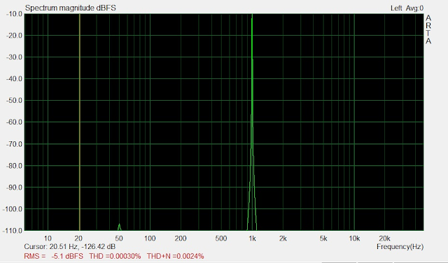
.png)


.png)


