Show by Label

Saturday, July 15, 2017

My New Power Supply Design Project Part 2

I actually built prototypes of the earliest design and started to learn more about the functionality, and try to find the limits. I'll go in much more details later, but for now let's go through the characterization of the complete control segments and see how stable this design rally is, by using the simulator. In the process, we will also figure out what frequency optimization we can use to make the supply stable and still have the optimum switching speed, which is the usual trade-off.

Because we are dealing with two circuits, the Voltage control and the current control, I have actually split the stability characterization in two parts.

Volt Control Stability Analysis and Tuning.

Here is the LTsim circuit of the Voltage control section:

I also use this for the Step Response measurements, so some artifacts are already in this schematic.  I won't go into many details because I may mislead you, but in order to do the stability analysis, you need to measure the Open Loop Gain. This is accomplished by "breaking" the Voltage feedback loop and inserting a small sweeped AC signal (V5 with 1V AC, 0 phase shift). 

In order to let LTsim establish the DC settings, we'll apply a huge inductor and a huge capacitor to block any AC from disturbing the Open Loop measurement. Because we want to do an AC analysis and get a Bode plot of the responses, we instruct LTsim to do an AC sweep with 10 decade steps from 10Hz to 100MHz. (.ac dec 10 10 100meg) as you can see below V1. (The .trans instruction below it is turned into a comment and does not play a role here.) I have isolated the Current Control section by breaking the connection between the LED and the bias circuit.
With a load of 10 Ohm at the output terminal we draw the maximum load (3A).

After I played with the frequency compensation networks (C7 R6) and a potential network across R8, this is the resulting Bode plot.


There are a number of key parameters to obtain from this plot.
1. The cross-over frequency (fx) where the Gain curve (straight line with scale on the left) is crossing the 0dB or Gain=1 line. In this case the frequency is almost 10KHz. This is a function of the speed of the system.
2. The Phase Margin. The phase curve is the dotted line with the scale on the right. This is a measure of the stability of the system. The Phase Margin (PM) should be >45 degrees at fx. In this case it is about 60 degrees, which is OK.
3. The Gain Margin (GM). The GM is another measure of the stability of the system. When the Phase is crossing -180 degrees, the system will oscillate. There should be enough margin in the Gain to prevent that. The GM at fx is about 50dB. The GM at -180 degrees is minimal, but the Gain is already attenuated with 100dB, and the Phase is crossing the -180 degree point at 50Mhz. I don't think this causes any harm.
4. The slope of the Gain at fx should be -20dB/decade, and that's exactly what is is.

I think that this is good enough to try in real life.

Current Control Stability Analysis and Tuning.

Here is the LTsim diagram for the Current Control section that I used.

I disconnected the Voltage Control section by removing the connection between the LED and the bias. In order to make the current section do something to drive the pass transistor, I used a separate Voltage source (V5), and set that to 0.1V, enough to drive the Current Limiting with 10 Ohm at the output. The Open Loop Gain is obtained by breaking the feed back loop with the same trick as I used for the Volt section.

Here is the resulting Bode plot.


Let's look at the 4 key criteria again:
1. fx at just over 400KHz, which is pretty fast. One of the reasons is that there is no large capacitance in this loop, because the output cap C6, is out of this loop.
2. PM at fx is about 65 degrees (-220 + -155), which is OK
3. GM at fx is about -40dB, which is OK
4. Slope of Gain at fx is about 34dB, also good.

Step Response Verification for the CV to CC/CL Mode Changes


This is the combined circuit of the two above. 


The difference is with the LTsim analysis instructions, because now we want to see the system in action. Three LTsim settings are needed. We tell the simulation to run a transient measurement by making the .trans instruction active again. We tell the simulator to run for 55mSec.

Because we want to see the Voltage turn on and off, we instruct V1, the volt setting input to start at 0V, after 5mS switch to 2.5V (which is 15V at the output), and leave it there for 40mSec. Both ramps are with 10uSec edges.
Because we want to see the Current limited in action, we set the current setting input V7 to initially start at 1V (no CL), after 15mSec, switch to 0.5V and leave it there for 10mSec. both edges are 1uSec.
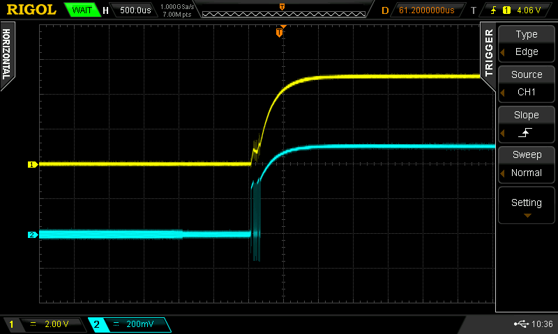
Here is the result:


At 5mSec, the output goes to 15V, at 15mSec, the CL kicks in. At 15V, a 10 Ohm resistor will result in 1.5A and with the CL set at 0.5V this will result in a maximum current of 226mA, causing the voltage to drop to 2V. The edges are very clean, no ringing, no overshoot. The round corner of the leading edge of the CL is die to the fact that the output capacitor is de-charging, causing a slight delay in the CL limiter. This is the major reason I like to keep this capacitor as small as possible, and I even put a small resistor in series. Real testing will reveal of this is acceptable or not.

Here is a trace of the current going through the load resistor:


The output current starts out with 0A, then switches to 1.5A. When the CL kicks-in the output goes to 226mA, after which it goes back to 1.5A, to become 0A again towards the end.


Thermal Protection & Management
Because I use rather small enclosures, the size of the heat sinks where the pass transistor(s) are mounted on are limited in size. The worse that can happen is when the series pass transistor develops a C-E short, which will surely destroy the DUT, and may even destroy the power supply itself.

For this power supply, I wanted to have two thermal protections. One that would react as fast as possible to the die temperature of the pass transistor(s). Another circuit would be to drive a fan to cool the heat sink, but I only want the fan on when it is needed, to cut down on the noise level. (I cannot stand loud fans!)

Let's cover the thermal protection of the pass transistor first. The easiest method I have found is to mount an NTC directly on top of the transistor. I have found an NTC that is mounted on a lug that can be inserted under the screw that mounts the TIP142 to the heatsink. I have found that the fastening screw itself gets warm very quickly, and since the NTC is also on top of the plastic package of the transistor, there is little mass involved, so the NTC will react pretty quickly.

I use a simple comparator circuit to set the trip temperature of the NTC.


Normally, the 10K NTC is part of a voltage divider, here with R1 and R2. I simulate the voltage level of this divider with V3. When the voltage is representing the right trip temperature, the Opamp switches state and sucks the bias current away from the pass transistor, turning it off. R5 is used to create a hysteresis so this switching state will not oscillate. You want to be able to turn the supply off, because it will otherwise turn on after the temperature has lowered. Sometimes that's OK, like if you are charging a cell.


Here is the resulting trace.  The green trace depics the voltage of the divider with the NTC, and this will turn on the Opamp, taking the bias current away. After the temperature has move up a bit higher than the trip temperature, the supply is turned on again.


Output Load
To add stability to the overall control loops, it is customary to add a little load to the output, so everything is under control when there is nothing connected to the output. You could simply use a resistor, and I have been using a 3K3 resistor so far, which generates about a 10mA current, at 30V. However, knowing Ohm's law, that load is dropping to about 1mA below 10V, so no longer really a load...

In many supplies, a constant current load is created by an LM317, or a J-FET. Unfortunately, these solutions only work well above a few Volts. I came across a simple and very effective circuit, unfortunately, I did not record where I found it. Apologies to the creator, because this is a very nifty circuit and starts working above about 0.6V already.

Here is the circuit as I tested it in LTspice: 
(actually I verified it again after I blew up the transistor on the PCB while I was ramping up the output voltage the first time.)


Four components is all it takes to create a constant current of 10-12mA, regardless of the output voltage.

Here is the simulation:


The red trace is the power supply output voltage that is going from 0 to -30V and back. The green trace is the current through R2, the 56Ohm resistor. The current flows when there is more than 0.6V, or thereabouts, on the output.

There is more to this circuit though... I initially build a prototype with normal THT components on a breadboard. I used a 2N3904 transistor (my favorite workhorse) and a BS170 MOSFET. I picked this MOSFET because I use that a lot and it was the first one I saw in my box. I tried it and was amazed how well it worked. Initially, I was going to use a single J-Fet, but I didn't have one that was capable of handling the 30V output voltage. I tried a few alternatives, but this is by far the best solution.

When I populated my PCB, I selected two SMD parts. A BC847B transistor and a 2SK3018 MOSFET. When I first tested the supply and started to ramp up the output, the transistor turned into a torch. It turned out that the 2SK3018 was not up to the task, because the VDS rating was too low. I sloppily selected this part, instead of a 2N7002 that I also had in my box. Because I did not take the trouble to simulate this with the actually selected components, I overlooked this fact. So to understand what was going on, I added the2SK3018 and the 2N7002 MOSFET 's to the LTsim library and did it again. Sure enough, the 2SK3018 caused the fail. After replacing both parts, everything worked as expected. Lesson learned!


Fan Controller
I also use a fan controller circuit, to turn the fan on and off, and the chip I use will control the speed of the fan based on the temperature. The NTC needed for this circuit is mounted directly on the heat sink with a bolt.

The chip I use to control the fan is the TC648B that I also used in other projects. Have a look at my other post for more information.


I'll continue in Part 3
http://www.paulvdiyblogs.net/2017/07/my-new-power-supply-design-project-part.html

If you like what you see, please support me by buying me a coffee: https://www.buymeacoffee.com/M9ouLVXBdw


Friday, July 14, 2017

My New Power Supply Design Project Part 1


Although I have been using my 0-30V 0-1 or 3Amp power supplies for quite some time now, I have never been really happy with them. They are described in other posts on my forum.

The major design constaint, in my opinion, has to do with the poor scaling of the circuit. It is not possible to go much above 30Volt at the output, because the raw input voltage will become too large for the maximum supply voltage of the used Opamps. Also, the current shunt is too big, causing a significant voltage drop in the ground circuit at higher loads. Also not very good. 
As I have shown in my forum post while trying to improve this design, a significant weakness of the design is that (deadly) transients can appear on the output when the main power is switched on and off. You need to go through some significant modifications to avoid this. Lastly, the reference voltage that is used for the voltage and current setting is simple, but not very quiet nor stable. This principle design is very popular and easy to build but dates back many years. It was designed with the 2N3055 as the pass transistor, which is notoriously slow. Lastly, it is not easy to modify this design to use digital controls, ie control the volt and current settings with a DAC.


I always wanted to build a supply myself, so after a lot of reading forum posts of designs, studying other designs DIY and commercial and several handbooks, I started to piece together what I wanted. BTW, an excellent reference is the "DC Power Supply Handbook" or Application Note 90B from Hewlett-Packard/Agilent Technologies. There are 3 versions of that App Note as far as I know. Google for it and you shall find. Figure 3 on page 19 of the B version shows the basic block diagram of the supply I want to build.

DISCLAIMER
I'm not a professional engineer, I'm a hobbyist. I do have an electronic education, but that formally ended in 1972. After I retired a number of years ago, I picked-up my old hobby and I have been learning ever since. I try to document what I'm doing for people that know as much as I do, or even less, that are trying to learn as well, so I try to keep it simple. I'm using simplistic terms and they may not always be totally correct and I won't go in the theory, nor will I explain everything I did. Please keep that in mind.

BTW, I did not design this Power Supply from scratch myself. It is a combination of various pieces I found over the last couple of years, and they are the result of much more qualified people. I only made some changes here and there or adjusted or modified something to suit my needs.

Design Goals
Before we dive in, I had set aside a couple of goals that I wanted this new supply to have, basically making a much improved version of the ones I already have (all described in other posts on this blog)
The first one was to eventually drive this supply with a micro controller. This would allow me to precisely set the voltage and current levels, but also combine the power supply with a new programmable DC Load and create a feed-back system for elaborate tests. 

This requirement puts some constraints on the way the Voltage and Current are to be set. I also wanted to use a much better reference voltage, to make the supply as quiet as I could, without going to extremes. I can't really measure that anyway. 

Yet another one was to make the analog and later digital controlling hardware as detached as possible from the power section. This allows me to use the same design with very different supply specifications. The reason is that I put my transformers in separate enclosures. Power transformers are expensive and bulky, and my bench space is precious and limited. The other power supplies I have follow the same principle. It allows me to switch raw supplies or upgrade transformers without rebuilding the complete power supply. The new basic controller architecture will allow me to go up to 100Volts or more if I want to, and 3, 5 or 10 Amps if needed.

The Basic Concept
To get started, let me explain the basic principle by using a simulator. I use LTspice.
Here is the basic concept:


The pass transistor, a TIP142 NPN Darlington transistor, is biased with a stable 10mA current. With this current applied, the transistor will be fully open, so the output voltage is the input voltage minus the drop of about 0.6V The bias is accomplished with V1 and I1. R3, the base resistor is needed to avoid oscillations, and needs to be as close as possible to the TIP142 transistor Base pin. The pass transistor is going to manage a raw power supply, V2, which is currently set to 10V.

The "Trick"
The "trick" to drive the TIP142 on and off is to actually "suck" the bias current away from the base. In this simulation example, that is accomplished by another voltage source, V3. Because we want a visual indication later on if the supply is in the Constant Voltage (CV) or Constant Current (CC) mode, we use an LED in series with a small current limiting resistor, R5. The voltage source V3 is simulating the Voltage setting circuit. In this case, we let the voltage step from 0V to -4V with a slow rise and fall time. Because the negative going voltage will source a current through the LED and R5, it will take something of the available constant current (10mA) away from the pass transistor, making it less conductive and hence limiting the output voltage.

The Floating auxiliary supplies
Note that for this circuit, all the controlling voltages are referenced to Vout+, which is tied to the ground level of the overall circuit. On the outside BNC connectors, this does not matter, because the negative output (Vout-) is the "ground" level to the outside world. So the negative output voltage, which will be the "zero" reference, is floating downwards. This construction is key to these kind of supplies and you really need to be able to wrap your mind around this before you can continue to follow and understand this architecture. If not clear, read the H-P app note I mentioned earlier.

So in essence, the auxiliary supplies for the controlling logic are floating on top (+5V) or below (-5V) the Vout+ supply, and this is accomplished by tying the ground of the auxiliary supplies to the Vout+ pole. Now you can probably already see why the raw supply can be 100V, because it does not matter for the controlling logic. It floats on whatever level of the raw voltage we select to use.

In any case, here is the result of the simulation:


The red trace is the result of V(set), the voltage source V3. The green trace is the output voltage, measured at the negative side of the output (Vout-) At about -2.7V of V3, the conductivity of the pass transistor is closing rapidly, and about 0.6V further down, the transistor is "closed", there is no output anymore. When Vset starts to rise again, the same happens in reverse. Look at this graph and the circuit until you really grasp what is going on.

Controlling the Constant Voltage Setting
The next step to control the above turn on/off process better is by using an Opamp that is more capable to open and close the transistor. By selecting an inverting Opamp, we get a positive going voltage setting resulting in a rising output voltage.  When we apply the resulting output (Vout-) to the Opamp, we give the Opamp the feedback to get a closed loop system. I specifically selected the TL071IP Opamp, because it is available in a DIP and SOIC version, dual and single Opamps per package, has J-Fet inputs and is generally speaking a very good Opamp. There many others to choose from, in most cases you will not really see any benefits or changes.

Here is the LTsim schematic:


A few things to note. I have raised to raw supply to 35V. This gives the series pass transistor some headroom for a 30V supply output. The Power Supply itself is really a high gain amplifier. It needs a capacitor (C1) on the output for several reasons. This capacitor should be as small as possible. The inverting Opamp has a small capacitor (C2) in the feedback to limit oscillation, and this turns it into an integrator as well. This capacitor could also be applied across the feedback resistor R4, or in a combination. We'll get to that later. The feedback resistor R4 has a value that limits the output of the supply to 30V. The combination of the voltage setting and the feedback is "summed" at the inverting input of the Opamp.

This is the result of the simulation:


The green trace is the result of the Voltage setting source V3, which is now going from 0 to +5V. This results in an output voltage (red trace) rising with the input voltage smoothly to the maximum output of 30V, and back again.
If we were to use a potmeter connected between ground and +5V, instead of V3, we could set the output precisely in the range from 0 to +30V, which is what we want.

Note that the voltage we feed into the summing input of the Opamp to set the output voltage, has a direct relationship (5V in = 30V out or 1:6), so every change due to noise or instability of the input voltage will have a direct influence on the output. From now on I will refer to this voltage as the Reference Voltage.

The reason I selected +/- 5V for the auxiliary supply is to accommodate a DAC and ADC later on.

Note that the only component that needs to change if you use a different raw voltage, is the feedback resistor R4.
This is an important step if you want to make a supply scale-able and universal.

Adding the Current Limiter
The next logical step will be to add a way to control the amount of current the supply can deliver to the output. The easiest method is to include a small (shunt) resistor in the output connection, and measure the voltage across it. When the voltage level across the shunt has reached a certain value, we want to limit a further rise.

Here is the LTsim circuit with the current limiter added:


The second Opamp measures the voltage across the current shunt resistor through R9, and compares that with the current limiter voltage reference V5. The current shunt should be as small as possible to avoid adding an influence and to limit the heat developed into it with high currents.
The principle is the same as with the voltage setting. When there is too much current, the second Opamp will start to suck the bias current away from the series transistor, and that will lower the conductivity, resulting in a lower output.

Because the voltage drop over the shunt is very low with only a 10mA load (the 3K3 resistor), I used some formulas in LTsim to lower the voltage setting and the voltage output, so you can see the relationship.

The purple trace is the voltage setting. It still goes from 0-5V, but the trace level is divided by 100 as you can see in the label. The green trace is the current level voltage, going from 10mV towards ground. The power supply output is the red trace, divided by 600 to show the relationship. You can see that the output is going back in step with the current setting voltage all the way to 0V when the current limiter is active. 

I already mentioned that the Reference Voltage is critical, and especially with the Current Limiter, which deals with milliVolts, this is even more critical. Another stability factor is the bias current level. When this fluctuates, the output cal fluctuate with it. Let's look at a simple circuit that will be an adequate constant current source.


The Bias Current Circuit

Here is the really simple circuit that will provide the bias current for the pass transistor.


A single transistor, two resistors and an LED is all that is needed. The LED is a red (3mm) version. The color can also be green, but stick to these two because of the voltage drop. With an emitter resistor (R1) of 220Ohm and a bias resistor (R2) of 5K6, you get a steady 8mA constant current at the collector. The type of transistor is not really important, I use a run of the mill 2N3906.

One important aspect of a power supply is the ability to switch it on and off with the main switch. You should never really do that, but as a minimum, there should be a form of protection, such that the supply does not harm your Device Under Test (DUT). Typically, when a supply is started up, the voltages for the various parts need to settle before regulation is stable. With this circuit, we can add a capacitor across the LED to delay the bias current for a few 100 milliseconds, so the other circuits have time to stabilize before the TIP142 gets turned on. I selected an electrolyte capacitor of 200uF. This will delay the turn on by approx. 1 second.

We will discuss the turn off protection later.


Main Power Off Protection
Just in case you switch off the Power Supply through the mains switch, or when there is a mains problem, you don't want the Power Supply to damage or destroy your DUT. You may have some expensive parts that your working with.

The turning off is a delicate and unstable process, due to the dwindling supplies. They may all act differently due to the load that the supply is feeding, and the capacitance reservoirs in the internal supply circuits. I have seen outputs of power supplies that shot op to several times the set output voltage, surely destroying delicate parts.

This supply was behaving rather well, but if you try long and hard enough, there will be situations where there is a large spike on the output. The following circuit makes sure that as soon as the main supply is decaying, the pass transistor is switched off, regardless of the state of the controlling logic. I spent quite some time finding and improving that circuit, and eventually settled on this:


I will show later that I use a small 9-0-9VAC transformer  to create the +/- 5V auxiliary supply voltages. The AC voltage is rectified and fed to 5V regulators. These typically have a 2V drop out, so they will certainly  regulate when the input voltage is above 7V. The rectified and buffered raw voltage is about 13V. This is simulated by V2, which is the input to the turn-off protection circuit.

The base of Q1 gets turned on when the voltage is that of the Zener diode (10V) plus the 0.6-0.8V of the Q1 junction, or at 10.8V. That turn off is amplified by Q2, which acts like a Schmitt-Trigger and further amplified by Q3. Q3 will turn on and start to sink the current from the bias circuit, turning the pass transistor fully off.


Here is the result. The green trace is the raw 13V supply. If that falls below 10.8V, the auxiliary supplies are still fully functioning, but Q1, Q2 and Q3 immediately sink the bias current away from the TIP142 to 0mA (the red trace) and so turn off the output.

I will continue in Part 2
http://www.paulvdiyblogs.net/2017/07/my-new-power-supply-design-part-2.html


If you like what you see, please support me by buying me a coffee: https://www.buymeacoffee.com/M9ouLVXBdw


Thursday, March 2, 2017

_HowTo: Move the filesystem to a USB drive/stick

This was actually my very first post on the raspberrypi.org forums.
It has been visited a million+ times, so it has been useful to many people.

I was honored when the forum guys selected this post as "sticky", making it easy to find.


Recently, I updated the procedure to more reflect the changes in Raspbian.

Here is the link : https://www.raspberrypi.org/forums/viewtopic.php?f=29&t=44177

Enjoy!

If you like what you see, please support me by buying me a coffee: https://www.buymeacoffee.com/M9ouLVXBdw

Monday, November 14, 2016

Demistifying Rotary Encoders (updated)


For an Arduino based project, I wanted to use a rotary decoder to control a menu based structure.

As you are probably aware, there are dozens of solutions available, typically one more complex than the other, in an attempt to make it reliable and fast.

There are basically three schools of thought. One set of die-hards believe in a pure software solution,  and others in a hardware solution, the remaining ones, the more practical ones?, use a combination of both.

Then there are two ways to get the information from the encoder. You obtain the switch recognition in the main loop construct, or you use 1 or 2 interrupts. In the first case, you need to carefully design the main loop, because if you don't get the timing right, the recognition of a twist (a click) of the decoder will be slow, or can be missed. This makes for a very poor user interface (U/I) because it does not seem responsive.

Using an interrupt to recognize movement can be more responsive, unfortunately, almost all interrupt based solutions use two interrupts. On the Arduino Nano or Mini-Pro, there are only two external interrupts available, so using both can be a problem. The good news is that you really don't always need two interrupts.

If you look at the datasheet, you are presented with perfectly modeled waveforms of the two switches that are central to these mechanical decoders. I'm not discussing the much more expensive optical versions here. Here is a picture of the typical waveforms.


Image result for rotary encoder switch


First off, the real wave-forms are not perfectly symmetrical, the output is depending on the mechanical construction and the rotation speed. The other important bit of information is that practically, you rotate the switch from indent to indent.

Here is a screen shot from a one indent move clockwise, captured with a Logic Analyzer:


And here is the screen shot of moving one indent anti-clockwise, or back.


Notice the different pulse width of the A and the B switches in both cases.

The challenge is to not only detect a rotation movement, a click, but also the direction, and then in such a way that you can also rotate the switch very fast and always be correct.

Using one interrupt

In the following Arduino sketch, I use one interrupt on the rising edge of the A-switch, and then sample the level of the B-switch. As you can see above, a clock-wise (to the right) rotation will cause the A-switch to become high before the B-switch. If you turn the other way, the B-switch is already high when the A-switch becomes high.

In order to track and visualize what is going on, I added some statements in the code that will generate a trigger pulse so the Logic Analyzer or scope will help us with the timing relationships.

Here is the sketch:

/* Software Debouncing - Mechanical Rotary Encoder */

#include <FaBoLCD_PCF8574.h>             //include the i2c bus interface and LCD driver code

//---- initialize the i2c/LCD library
FaBoLCD_PCF8574 lcd;                     //with this, there are no further code changes writing to the LCD

#define encoderPinA 2                    //encoder switch A
#define encoderPinB 4                    //encoder switch B
#define encoderPushButton  5             //encoder push button switch
#define Trigger 6                        //Trigger port for Logic Analyzer or Scope

volatile int encoderPos = 0;
volatile int oldencoderPos = 0;

void setup() {
  pinMode(Trigger, OUTPUT);
  pinMode(encoderPinA, INPUT);
  pinMode(encoderPinB, INPUT);
  pinMode(encoderPushButton, INPUT); 
  attachInterrupt(digitalPinToInterrupt(encoderPinA), rotEncoder, RISING); //int 0 
  lcd.begin(16, 2);                      //set up the LCD's number of columns and rows
  lcd.clear();                           //clear dislay
  lcd.setCursor(0,0);                    //set LCD cursor to column 0, row O (start of first line)
  lcd.print("Rotary Encoder");
  lcd.setCursor(0,1);                    //set LCD cursor to column 0, row 1 (start of second line)
  lcd.print(encoderPos);
}

void rotEncoder(){
  boolean rotate;
  delayMicroseconds(300);                //approx. 0.75 mSec to get past any bounce
                                         //delay() does not work in an ISR
  //send entry Trigger pulse
  digitalWrite(Trigger, HIGH);
  delayMicroseconds(10);
  digitalWrite(Trigger, LOW);
 
  rotate = digitalRead(encoderPinA);           //Read the A-switch again
  if (rotate == HIGH) {                        //if still High, knob was really turned
    if (rotate == digitalRead(encoderPinB)) {  //determine the direction by looking at B
      encoderPos--;
    } else {                                  
      encoderPos++;
    }
  }
  //send exit Trigger pulse
  digitalWrite(Trigger, HIGH);
  delayMicroseconds(10);
  digitalWrite(Trigger, LOW); 
}


void loop() {
  //loop until we get an interrupt that will change the encoder position counter
  if (encoderPos != oldencoderPos) {
    lcd.setCursor(0,1);
    lcd.print(encoderPos);
    lcd.print("      ");
    oldencoderPos = encoderPos;
  }
}

And here is a screen shot of a forward indent with the trigger pulses:


As you can see from this data, it takes the Arduino 755 uSec from the A-switch rising edge recognition to the entry into the Interrupt Service Routine (ISR). It then only needs 14.2 uSec to do the rotation recognition.

To put this into perspective, so you get an idea of the relative "blinding" speed of a 16MHz Arduino in relation to slow moving switches:


 Turning the knob as fast as I can produces the picture below:


This solution works pretty good, but is not perfect.

A more reliable method, using two interrupts

This is my most favorite solution. I have used this method with a lot of success, but it uses two interrupts to determine the direction and the clicks. Unfortunately, the number of interrupts on the Arduino is limited, so you may not always have the room to implement this.

In the global area, you need this:

// Rotary Encoder setup
static int enc_A = 2; // D2 No filter caps used!
static int enc_B = 3; // D3 No filter caps used!
static int enc_But = 7; // D7 No filter caps used!
volatile byte aFlag = 0; // expecting a rising edge on pinA encoder has arrived at a detent
volatile byte bFlag = 0; // expecting a rising edge on pinB encoder has arrived at a detent (opposite direction to when aFlag is set)
volatile byte encoderPos = 0; //current value of encoder position (0-255). Change to int or uin16_t for larger values
volatile byte oldEncPos = 0; //stores the last encoder position to see if it has changed
volatile byte reading = 0; //store the direct values we read from our interrupt pins before checking to see if we have moved a whole detent


In the setup code, you need this:

  // setup the rotary encoder switches and ISR's
  pinMode(enc_A, INPUT_PULLUP); // set pinA as an input, pulled HIGH
  pinMode(enc_B, INPUT_PULLUP); // set pinB as an input, pulled HIGH
  attachInterrupt(0, enc_a_isr,RISING);
  attachInterrupt(1, enc_b_isr,RISING);


Here are the two Interrupt Service Routines, one for each switch:

/*
 * Rotary decoder ISR's for the A and B switch activities.
 */
void enc_a_isr(){
  cli(); //stop interrupts
  reading = PIND & 0xC; // read all eight pin values then strip away all but pinA and pinB's values
  if(reading == B00001100 && aFlag) { //check that we have both pins at detent (HIGH) and that we are expecting detent on this pin's rising edge
    if (encoderPos <= 0){
      encoderPos = 0;
    }else{
      encoderPos --;
    }
    bFlag = 0; //reset flags
    aFlag = 0; //reset flags
  }
  else if (reading == B00000100) bFlag = 1; //we're expecting pinB to signal the transition to detent from free rotation
  sei(); //restart interrupts
}

void enc_b_isr(){
  cli(); //stop interrupts
  reading = PIND & 0xC; //read all eight pin values then strip away all but pinA and pinB's values
  if (reading == B00001100 && bFlag) { //check that we have both pins at detent (HIGH) and that we are expecting detent on this pin's rising edge
    if (encoderPos >= 255){
      encoderPos = 255;
    }else{
      encoderPos ++;
    }
    bFlag = 0; //reset flags
    aFlag = 0; //reset flags
  }
  else if (reading == B00001000) aFlag = 1; //we're expecting pinA to signal the transition to detent from free rotation
  sei(); //restart interrupts
}

This is a much better solution, and even needs no extra hardware parts. I have not been able to detect any false "claims". However, I have not tried it on faster processors so be aware. 

In the meantime, I modified this code to add acceleration, and used it on an ESP32. The code and details can be found in my DC Dynamic Load project here.

There are other debounce solutions in software that only use one interrupt. And then there are solutions that rely on the fact that if you trigger on the edge of one of the pins, the level on the other pin is in the middle of it's cycle and therefore stable. If you "transpose" that level in place of the one you triggered on, you have effectively eliminated the bounce. Very clever! Have a look here : Special Solution


Rotary Encoder with hardware debounce en direction decode

The following is an attempt that uses hardware debounce en encoding to reduce the processing overhead (less false triggers) and can be used on the 8 or 16MHz clocked Arduino's, and also with faster processors like the Raspberry Pi or the ESP processors.

Here is the schematic diagram.


The idea is to determine the direction with the aid of a Flip-Flop. First the switches are debounced with an R/C combination and then fed to Schmitt-triggers to get clean logic transitions again, This circuit creates a clock pulse for every indent and a directional level that changes only when the direction changes from clockwise to anti-clockwise. 

I created a small PCB, and here is the result of my soldering.


However, is it perfect? Unfortunately no. The switches of very cheap China rotary encoders as the one above are mechanically inferior, but really good ones, typically the optical kind, are expensive. After some testing, I reduced the values of the capacitors to 10nF. In combination with the 10K resistors they are sufficient.

This extra hardware reduces a lot of processing power for the micro-controller, because it reduces the amount of false triggers and is not relying on interrupts, although you could use one on the CLK signal. It could be used in a polling loop as well.

However, when you have bounces like the ones below, all bets are off. These are taken from a cheap no-name rotary switch. In this case, I just used a 10K pull-up resistor to 5V to the switching pin and used GND on the common pin.


Below is an example with a simple and typical 10K/10K/10nF r/c filter like the one in the schematic diagram above. It adequately filters out most of the bounce noise. This is actually taken from an ALPS STEC12E08 version, which is a lot better than the cheap no-name ones. At €2,34 its not that expensive.


However, even these much better quality rotary switches are not perfect, see below. The blue trace is taken directly from the switch, the yellow trace after the simple debounce circuit. In my opinion, the only solution in that case is to use a combined hardware/software solution. You would have to use pretty long delays after the trigger to attempt a software solution. 


It shows that you cannot simply use one-fits-all solutions, you really should try it out, based on your switch and your application.


If you like what you see, please support me by buying me a coffee: https://www.buymeacoffee.com/M9ouLVXBdw


Sunday, October 2, 2016

Building a Bench Tracking Dual Voltage Supply


Dual Tracking +/- 30V @ 100mA Power Supply


While I was building this supply, I added some functionality but did not update the front panel. That's why you see the pen markings to indicate the switch position for the DMM display measuring the positive supply or the negative supply, and that the Tracking switch puts the positive supply in the Master role. The "S" means separate supply adjustments.

The PWR switch is not a main power switch, but removes the voltages from the output to protect the DUT. It also allows you to set the voltages of the supply without having to take the leads away from the DUT. The switch should have "on" and "off" labels.

My Design Goals


For some of my experiments and tinkering, mostly with op-amps, I wanted to have an additional power supply that would give me a precise dual-tracking complimentary voltages, up to +/- 30V.

Here are a few design goals I set for myself:

1. True 0 to +/- 30V.
2. Non tracking mode to set two different voltages for the negative and the positive supplies.
3. Precise dual tracking within 1% or better.
4. Precise Voltage level setting with 1mV accuracy
5. Accurate display of output Voltages with less than 0.01% error. (no need fro an additional DMM)
6. Pretty good current limiting setting with a visual indicator. (not at a precise exact value, but good  enough because I don't want to blow-up an expensive device.)
7. Pretty good constant current/voltage operation.
8. Low noise and stability without going to extremes.
9. Small package, using the same housing as several of my other supplies and DC Load.
10. Maximum current of at least 100mA for each supply separately.
11. Using components like voltage display and transformers to be used with a drastically different design. (just in case I wanted something complete different)
12. Some protection against blowing things up and doing stupid things myself.

Using standard Regulators

For a while, I was contemplating a simple tracking LM317/337 supply, and I looked around of what designs where out there on the Web. There were surprisingly few, actually, and none fitted my bill.
Eventually, I started to piece some things together myself, but by the time I added the bells and whistles I wanted, things were getting complicated quickly.  Rather than scrapping the whole idea, I continued as a learning experience to see how far I could get this to work. In the back of my mind however, I always considered starting all over with a more traditional supply design, so I made sure most of the more expensive components could be re-used.

Here is the circuit diagram of the complete supply. Looks pretty wild when you look at it initially, but when I'll go through the building blocks it's actually not that bad. 


Let's just start with a partial diagram of the positive supply, and dive right in. 


Voltage Regulation

The output voltage is regulated and set by IC7, an LM317AHVT, which is the high voltage version of the LM317 regulator. To get a regulated 30V at the output, I need to supply several volts more. When the transformer is not loaded much, the input voltage can get to levels that are too high for the standard LM317, which is why I use the "HV" (High Voltage) version.

R28 is used in combination with R27, the 10 Turn potmeter to set the output level. R28 also makes sure that there is some minimum current flowing to keep the regulation in check. That only works well with higher output voltages, so I use a J-FET, Q5, used here as a constant current source, to ensure that the LM317 always sees an 8mA or higher current. The J-FET needs a few volt to work with, and I decided to give it -8V, because I can use that voltage level in other places as well.

The voltage adjustment setting is stabilized with C17, but that means that you also need D17, to protect the LM from the C17 discharge levels going the wrong way. To make sure that I can regulate down to 0V, I have to overcome the reference voltage of the LM317, which is 1.25V. Initially, I used a -1.25V voltage reference to create that counter-balance, but I was not too happy with how that worked. D25 and D26 in combination with the -8V will do the same and actually clamp the negative supply at the Source of Q5 to about -1.3V. That's close enough. 

Current Regulation

Let's switch our attention to the current regulation/limiting section. IC4, yet another LM317 is used as the current limiting device. The current limiting is depending on the voltage over the current shunt resistor, R12. The 12 Ohm value will limit the current to a maximum of 104mA. To make that current start from 0mA, I used the same circuit around D13, Q2 and the negative supply of -8V to do that. The variable current limiting settings are accomplished with a normal 1 turn potmeter R17, in combination with R16, to make the potmeter effective over the complete range of at least 100mA. D11 and D12 limit that range to about 1.3V, and that creates a pretty accurate way of setting the current limit. Q2, another J-FET, also functions here as a constant current source of about 8 mA, keeping IC4 into regulation at all times.

Current Limit Indicator

To get an indication of the entering into the Current Limiting or Constant Current mode, I used the circuit with Q3 and a red LED. Q3 measures the voltage drop over the LM317, and if it goes over a certain level (> 0.6V, when the limiting gets tripped), the LED with be turned on. Simple but effective.

The Negative Supply

The negative supply is a virtual mirror image of the positive supply. If you now look at the equivalent circuit on the negative side, around IC6, an LM377T, you'll see exactly the same circuit, with the Tracking Switch S2 in the position shown. Because IC6, the LM377, does not come in a high voltage version, I had to use another LM377 (IC3) as a pre-regulator to limit the voltage going in to IC6. IC3 limits the maximum voltage of about -40V to a -36V level which is safe for the 377 and provides plenty regulation head-room. Using another LM377 may look like an overkill, but the 5 components (The 377, a protection diode, two resistors and a capacitor) costs are really minimal. Yes I could have used D14 to go across all three LM377's, but that's the way the circuit developed.

Output Voltage Removal

In order to quickly remove the output level of the supply, I use a switch (S3) across both the Volt Adjustment potmeters, to do that. Eliminating the voltage over the potmeters will force the LM317/337 outputs to zero volt. And that pretty much covers the voltage regulation parts.

Dual Voltage Tracking

OK, let's move our attention to the dual voltage tracking circuit. I used a simple method with two precisely matched 10K resistors (R29 and R31) to create a virtual ground level at the midpoint. After testing the result, I found that I still needed an adjustment trimmer R30. The virtual ground or mid-point level at the wiper goes to the inverting input of op-amp IC8, and that compares that input with the true ground. There is nu current flowing so R10, the 4K7 resistor will not cause a voltage drop. The op-amp will make sure that it's output is driven such that the two inputs are equal. The output goes to the Tracking On/Off switch, and when that is flipped, it actually takes over from the potmeter setting of the negative supply, making that a Slave of the positive supply, the Master. The negative supply will now follow (track) the output level of the positive supply, also when the positive supply goes into current limiting. I have selected the TLE2141 op-amp for this job, because it can handle the supply voltages of -36V plus +8V = 44V.

The positive and negative outputs have C22/C23 and C18/C24 to filter unwanted noise. I kept C23/C24 as low as possible to protect the dumping of their capacity into my precious DUT circuit. This is a significant and often overlooked factor of most power supplies. 

Some Protection

D15 for the positive supply and D14 and D5 for the negative supply are there to protect the regulators in case the output voltage is higher than the set voltage. These diodes then dump the over-voltage into the main reservoir capacitors C6 and C5. This situation can happen when there are capacitors or batteries in the DUT that want to dump their charge back into the supply. They are protection for the LM317/337 devices. D18 and D19 are protection for reverse voltages that may accidentally try to dump into the supply.

The Supporting Cast

The supporting team is made up of transformer TR1 to supply the main voltage of the supply. Initially, I used R2 which is a PTC to add a level of protection for over currents. They are self-healing. After using the supply for a while, I took it out of circuit because it interrupted too early and I didn't have other values.

The main supplies are rectified with a full bridge filtered by reservoirs C6/C5 and C12/C9 to remove high frequency noise. Both R7 and R6 make sure that the reservoirs are emptied relatively quickly, so no voltages are present for very long when the mains is switched off. They will also put a minimum load on the transformer to protect for voltages that may become too high when there is no load supplied to the DUT.

To minimize the development of heat and use normal TO-92 regulators for the +/- 8volt supplies, I used a separate transformer with 9-0-9VAC at 80mA. These print transformers are relatively inexpensive and small, and the +/- 8V supplies are now independent of any voltage swings on the main supply. The filter circuits around IC1 and IC2 are text book stuff.

The Voltage Display

The last element is the voltage display. I found a module that has a real DMM "inside", is very accurate and works up to 33VSearch for: 0.36" 5-digit DC 0-33.000V Digital LED Voltage Meter

These displays typically generate a lot of switching noise that you really don't want to have injected into the power supply rails. At the same time, I wanted to use this voltmeter to measure the positive supply as well as the negative supply. Unfortunately, these meters only handle positive voltages. In order to switch the volt meter from one output to the other, the power for the meter needed to be floating from the main power. So, I needed a third transformer with 9VAC, to isolate the power rails and I could then do the switching with S1. S1 applies the positive output voltage to the plus input and the ground to the minus input, and reverses this for the negative supply (positive input is now ground, and the input ground is now the minus output supply. Simple and effective at only the cost of a little transformer.

Tracking Mode Side-Effect

There is one caveat with a tracking supply like this one. The negative supply (Slave) tracks the positive one (the Master). If the current limiting for the positive supply kicks in, the negative supply will follow. However, when the current limit for the negative supply kicks in, the positive supply will stay at it's set level, creating an unbalanced output situation. I have not figured out a way to solve that.

Real-Life Experiences

After I finished building the supply, have been using it for a few years now, and I'm very happy with it. The voltage level shown on the display is very accurate, it really acts like a good DMM, and so is the tracking accuracy which is well below 0.1%. During my experimenting, I find myself grabbing this supply more and more, even though I sometimes find the output dropping because I pull too much current from it. 

Below is a picture of the main circuit board in an earlier stage, when I was still using the 1.25V references (the SMD parts on the carriers), and without the current limit indicators. It has been modified quite a bit since then.

All parts within the dotted rectangles on the circuit diagram are mounted on the metal back-panel of the enclosure. The last addition, the third transformer for the display is mounted on the top half of the enclosure because I didn't have the room on the circuit board.

Sorry for the bad focus, but you get the idea.


Enjoy!


If you like what you see, please support me by buying me a coffee: https://www.buymeacoffee.com/M9ouLVXBdw


Friday, September 30, 2016

Building a Milli-Ohm Meter


This is a project to build a simple instrument to measure low value resistors below 2 Ohm down to the milli-ohms with a very high precision.


I already mentioned the SCULLYCOM Youtube series from Louis Scully, and a while ago I prototyped this design to see how well it would fit my needs. Here are his Youtube videos.

Build a Milliohm Meter
Update

Below is my circuit of the prototype I built, based on the first video.

Initially, since I used my DMM as a display, I also did not use the x10 multiplier. I was so happy with the accuracy that I decided to build the real thing, so I ordered and added the INA106, because it makes the read-out a bit easier without having to do the math.

The unit worked very well, even as a prototype, using my DMM as the display. The initial testing shows it to be very useful. When I found out that Greg Christenson (the same one from the Milli-Voltmeter PCB), also created a PCB for this project, I was sold and decided to built one based on his PCB. This is detailed in the update.

Here is his Greg's website: 
https://www.barbouri.com/2016/10/09/milliohm-meter-version-1-5/#more-413

This project is also a work in progress for me, because I'm still building my BOM to be able to order the required parts when I'm back home.

Here is Greg's version of the circuit diagram, that I will use as the reference for the BOM.


The BOM for this project, using mostly UK suppliers, is now available here:  BOM
And also on Greg's site here : BOM2

I use Mouser and/or DigiKey myself, because Farnell and the likes do not want to sell to hobbyists in my and other countries. Many alternative suppliers do not have some of these parts available. You can use several of the Farnell part numbers that Louis provided to look up parts with Mouser, and otherwise the description will help. There are some price differences with Mouser and DigiKey parts, most are less expensive, some significantly so, especially the 0.1% 25PPM resistors.

The PCB itself can be ordered here : PCB

Note that there have been a number of revisions, currently at 1.5, and there may be more.

Here is some information about the above parts:

C1..4 (22uF/25V) have some physical restraints to fit on the PCB. The dimensions are diameter 5mm, height 7mm (not so critical), lead space 2mm.

C5 (can be 150, 220, 470 or 1000uF/35V) and also has some restraints. The dimensions are diameter 10mm, height 12,5mm(not so critical), lead space 5mm.

IC2 and IC5 are from Linear Technology and Mouser does not carry that brand. In that case, I usually mix my order between Mouser and DigiKey and keep an eye on the free shipping limit of 50 Euro's or more. The IST version of IC2, the LT3092, is the preferred version, because it has better specifications.

Resistors R1 through R9 determine the constant current of 100mA. A precise and clean current is the Achilles heel for the design of this meter. There are four options for R2, 3, 4 and 5.  Louis has the Welwyn RC55Y series listed, but they cost a whopping 2.56 Euro's a piece. He also has the Holsworthy H856 series listed and they cost 1.72 Euro's. Mouser has the Neohm types as an alternative available. They have exactly the same specifications in term of precision (0.1%) and are also 15 PPM/C grade, however, the other two may have other better specs in general. There is a price difference though. The NEOHM version for R1 is YR1B63R4CC, and for R2..R5 is YR1B56R24CC, and they cost about 0.20 to 0.25 Euro each, depending on the value. Greg, the maker of the PCB, uses Vishay resistors from the MRS25000 series. They only have 1% precision and a TC of 50PPM/K. They cost 0.27 Euro's each. To get the required specification, he ordered a large number and selected the best ones.
Up to you to decide if your budget allows it and if you really need that little bit extra.

R12 and R13, the adjustment trimmers are quite special physically, so make sure you order the right type: 3296P-1-104F and 3296-1-101LF. There is also a 3366 version available that looks the same but is a little smaller and also seems to fit the PCB layout. (on the revision 1.5, Greg used both types as you can see from the pictures)

I have not decided myself yet if I will use the LCD meter as a display, or continue with using one of my other DMM's to display the value. The 6.5 digit Milli-Volt Meter, also designed by Louis that I'm building as well would be perfect for this job. Because I will only occasionally have a need for the milli-Ohm meter, a dedicated and rather pricey panel meter seems like a waist to me and also makes the enclosure larger. Besides, I have had some bad experiences of the LCD driver switching noise coming from these displays getting injected to my critical signals.

This decision will determine what enclosure I will use, but that will have to wait until I have the PCB and tested some things. The added benefit of using another DMM for display is that the panel meter  Louis selected only goes to 2V, and that limits the maximum value of the resistor you can measure to a maximum of 2 Ohm.

In the end, I decided to put it in a simple enclosure, use my DMM instead of a dedicated display. I'm not using it so often enough so that it warrants a dedicated display.

The 9V battery is a re-chargeable one.


The shielded DMM leads plug directly into my DMM.

I used my 6.5 digit DMM and was able to adjust the current to 100.002mA.

Testing a few reference value shunt resistors showed very precise measurements. My 6.5 digit DMM cannot measure this low and accurate by a long shot. However, it functions perfectly as a display for the instrument, showing the DC voltage that is representing the value of the resistor. 

This is a very nice tool to have in your collection. Highly recommended!


If you like what you see, please support me by buying me a coffee: https://www.buymeacoffee.com/M9ouLVXBdw