I finally got around to building my own DC Power Load.
My noise problems with the DC Power Supply, as described in
another post, forced me to build this tool so I could measure the results.
There are many designs on the web if you care to take a
look, but very few had a dynamic load feature, which is what I wanted.
I finally settled on one particular design and modified that
through some trial and errors. Here is my starting point that I got from the
work of Peter Oakes:
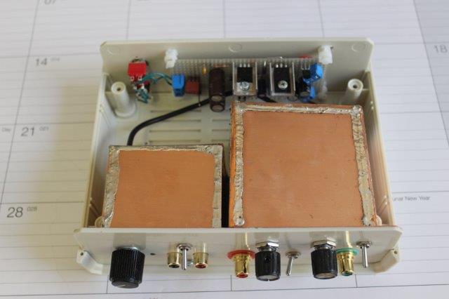
Here is my version:
Let’s go over the basic building blocks.
In order to have a stable setting of the load, independent
of supply voltage changes, I decided to use a voltage reference chip. The
voltage output of the chip was selected based on the maximum current I wanted
to sink which is 5 Amps. By using a shunt of 0.1Ohm, 5 Amps translates into
500mV.
So I selected an LM 358 with 1.25V output. By using a
resistor divider together with the current setting pot meter, I created a 500mV
level, so the pot meter could supply 0..500mV, or 0..5Amps.
By just changing just one resistor, I can later change the
load current to a maximum level of 12.5A.
The voltage over the shunt is fed to the negative input of U1,
which will try to keep this input equal to the positive input that gets the
desired reference voltage, by varying the output. The output of the Op Amp is
connected to a MOSFET that can handle plenty of Volts, Amps and Watts.
To set the current sink, or the load, I used the output of
the current setting pot meter and used a toggle switch to feed that to the Voltmeter
of my display. The voltage from the pot meter in milli Volts corresponds directly
to the current in Amps. (I first used a 10x op amp to convert the current to
volts 1:1, but that’s overkill of you can multiply by 10 yourself)
As I learned with my power supply project, these Volt/Amp displays
inject a lot of noise into the supply, so I used a series resistor, Zener and two
capacitors to stop that from entering the rest of the circuit.
If S3 is in the Direct setting, the reference voltage of the
pot meter is fed into the op amp. In the Dynamic setting I use a separate input
coming from a function generator or equivalent, in order to pulse the load at
certain frequencies. This allows you to measure the rise and fall times or
other responses of the supply under test.
To eliminate possible oscillations and to add stability, C7,
C3, C2 were added. I also created a possibility to add a capacitor parallel to
R4, to better drive the MOSFET, but did not need it at the moment. A Sobel filter
circuit was added at the output terminals for the same reason.
Unfortunately, the Volt/Amp display unit I have does not
allow floating measurements, which is why I had to put the shunt into the
ground loop. This will add a rather small (25mOhm shunt) current error.
I have another V/A display on order
that can be modified to make the current
measurement floating, which also allows high-side current shunts, which are
better anyway. Again Peter Oakes is the one that figured this out.
https://www.youtube.com/watch?v=A6VQhDioz_Q
In any case that current shunt of the modified meter can be
placed between the Drain of Q1 and the 0.1 Ohm shunt.
The Gate of the MOSFET is “clamped” to ground by a small
resistor, just to make sure a problem does not create an unexpected short to
the output. This resistor should be soldered right on the pins of the MOSFET
and the shunt, to take care of bad or broken wiring.
By using the dynamic load, I was able to measure a rise and
fall time of less than 50uSec, more than adequate for my applications.
One word of caution.
The MOSFET is capable of 55V, 110A and
200W. With 30V and a couple of Amps, it does not even get warm on my rather
small heat sink. The on resistance is only 8 milli Ohm, although we will never
get that low because we don’t saturate the device. However, dealing with higher
voltages and or higher currents increases the number of Watts rapidly. Remember
that the two multiply!


Update : Aug 29, 2015
Over the last couple of weeks, several things have changed after the initial build. I received my new Volt/Amp meter, and modified that per the instructions by Peter Oakes. It now has a floating differential current sense circuit so I have put it in between the MOSFET's and the current sense shunt. I'm also very impressed with the accuracy of both meters. No more adjusting, and the decimal point and number of digits change like a "real" DMM, what it really is. On top of that, it has exactly the same accuracy as my DMM. Highly recommended!
I also installed a temperature controlled fan, it uses a nifty fan controller chip to do all that. Look at a separate post for details.
To get a better handle on the temperature at higher loads, I decided to use two MOSFET's in parallel. I was a little careless testing all this, thinking that this plus the fan would solve my heat problems. I was eager to start my tests of the two PSU's, which is why I built this tool in the first place. Well, I lost a MOSFET due to runaway thermal issues. Bummer!
Despite my search for information on how to put two power MOSFET's in parallel, all I could find (at the time), was the use of seperate gate resistors, to balance the two MOSFET's. Well, that didn't work very well. Due to the differences in the VGS for both devices, one took all the heat.
After swapping out the broken one, I was a little bit more careful, and noticed right away that there was a large difference in the thermal balance between the two. One was getting slightly warm, but the other too hot to touch. Apparently, the only real solution to the RDS(on) and therefore thermal balance issue is to build two circuits with separate op amps and sense resistors. I did not want to do that right away, and tried to see if I could get close enough. First I increased the value of the gate resistors, and also matched them to within 1 Ohm. That did not do anything to get a better balance. I then started to increase the value of the one one that got hot, but that did not produce the result I was after. In the end I used a 10K trimpot to set the VGS to a reduced level, and used my temperature probe to balance the two. I got to within a few degrees C after running the unit with a 1A load, such that the temperature was about 50 degrees C. It's not ideal, because I don't think the VGS delta has a linear relationship, but for now I'm happy.
Here is revision 3:
This design will most likely be further tuned while I'm going through the paces of testing and specifying my two power supplies, so stay tuned.
Update : August 30, 2015
Well, it didn't take too long for another refinement.
I kept mulling about the thermal balance challenge, and was not too happy about the comment I made earlier in the post above. While surfing for ideas for the parallel use of the power MOSFET's, I came across a comment that I took for face value, assuming the guy knew what he was talking about. I simply repeated his comment in the previous post that the "real" solution is to make two separate circuits. So to duplicate the op amp, FET and current sense resistor.
I kept thinking about that statement, and decided that it is misleading or even incorrect. Yes, you will get two circuits that together will share the load, but it does absolutely nothing to get a better load balance, or a better thermal balance. So, back to the drawing board.
Initially, I wanted to use two thermistors (or NTC's), thermally connected to each FET, and then use a comparator to decide if one was getting hotter than the other. The challenge was that I could not find an easy way to mount them on top of the MOSTFET's. Sure, I could have mounted them on the heatsink, but I would have lost some temperature sensitivity, with the heatsink acting as a dampener.
I then switched to using the junction temperature of transistors, but again could not find a good thermal connection to the FET's. I then went through my power transistor stack for ideas and found two excellent specimens. I happen to have quite some (very old, as in late 1970's) D40C5 darlington power transistors, that have a very flimsy heatsink. This turned out to be a perfect way to mount them with the same screw that also mounts the MOSFET, provided you also isolate the transistor tab, because it is the collector. I happen to have all the bits and bobs required, so I could continue.
BTW, the fact that I use darlington transistors, is only because I had them. You can use any TO22X kind of package, as long is you can thermally connect them to the MOSFET's.
In any case, whipping-up a small circuit to measure the delta temperature difference and drive a FET to drop the VGS on the gate of the FET that get's too hot was quite simple. By selecting a feedback resistor to create a small threshold, I managed to keep the temperatures within about 1 degree C. So whenever the temperature of Q2 id one degree C higher than that of Q1, the gate of Q2 is clamped and as soon as the temperatures are equal again, the gate is released again. Perfect!
Here is Revision 4:
Resistor R21 in the drain of the BS170 MOSFET is there to reduce the gate voltage, not to yank it to ground. With the resistor combination of R9, R14 and R21, the gate voltage drops from about 300mV, just reducing the load and therefore temperature of Q2, while not affecting Q1, and therefore the output.
Just in case you are interested to use this idea in other applications, you need to be aware of two constraints. With this particular application, I'm not concerned about the self-heating of T1 and T2. I'm interested in the delta temperature difference, not the absolute difference. Also, the fact that the load will move from both MOSFET's to mostly one for shorter periods is of little concern for me. Both MOSFET's are individually capable of handling the full load.
Enjoy!
After having used the DC load for about a year, I was a little annoyed about the fact that I could not obtain a zero load at the output, despite the trimmer on IC1 and using a small negative voltage for it. Although the potmeter (R6) was getting down to zero Volt, the output of IC1 remained at 3V3, resulting in a 0.0059 Volt over the shunt (R12).
I finally figured out a way to adjust the potmeter range at the lowest position to have an output of zero load. The trick was to apply a very small negative voltage at the lower part of R6, instead of connecting that to ground. I used a tap on the two diodes that created a small negative voltage for IC1, in an earlier attempt to obtain a zero Volt output, and fed that -0.7V to an added 10K trimmer. With R6 in the lowest position, the new trimmer is now adjusted such that the output is showing no load.
Here is the new schematic with that change:
June 13 2017
While going through the design of a new power supply (a new post will be coming), I was not satisfied with the dynamic switching of the load. The pulse that is coming in from the BNC input actually switches the load hard on and off, so the maximum load is used, and there is no way to limit that.
I also didn't really need a fully variable input to the load, a simple pulse would suffice. During the power supply design, I actually put a 555 based timer on a breadboard and fed that to the DC load external input. I also added a few parts to make the output variable. I liked the results, so I put everything on a little prototype board and added it to the internals of the DC load.
Here is the schematic of the Pulse Generator addition:
Those that follow my posts will notice that I no longer use Eagle. A few months ago, I switched to Diptrace. I finally ended up frustrated by the difficulty in Eagle of adding custom parts, so I started to look around. I dismissed all the free ones, including K-Cad. That is just too cumbersome, and at this moment only for experts I think. An electronic pen-pal advised me to try Diptrace, and I have been using that ever since. My new power supply, discussed in another post has been designed that way, and I also made my very first pcb layout with it.
Anyway, I made Diptrace resemble the Eagle schematics a bit, because those still look visually pleasing.
OK, back to the Pulse Generator. I used a 555 based circuit that produces a pulse train with approx. 180mSec on, and approx. 70 mSec off periods. By just changing C3, you can change the frequency. At first, I used the 12V supply to power this circuit, but later changed my mind about that. I didn't want pulses with a 12Vp-p output roaring through my box, when I do sensitive measurements.
I changed the single throw switch that selected between static and dynamic inputs, to a double throw switch. The other side now switches the pulses off, by shorting the charging cap C3 to ground, such that the 555 pulses are off when the static mode is selected. It keeps things more quiet in the box. At first I switched the power to the 555, but turning it on produced an unwanted output glitch causing a high load on the output until the 555 settles.
The DC load will be switched on during the on-pulse, and fully off during the off-pulse. Because of the 5V supply, the output of the 555 timer is about 5V p-p. That signal is used for a trigger out signal. That signal now goes to the same BNC that was previously used as a pulse input. This signal typically goes to a scope to trigger it. This trigger output is an important feature because if you test a power supply, as an example, you want to see the effects of the load regulation while you switch dynamic loads on the power supply output. If the load regulation is any good, it will be very hard to see any effects on the output of the supply, so knowing where to look, based on the trigger signal, really helps a lot.
A second divider (R5 and the potmeter R6) attenuate the signal, so at the wiper of the potmeter, I will have 500mVp-p at maximum, and 0Vp-p at the minimum. A voltage level of 500mVp-p will turn the DC load fully on, which is the same as the static load adjustment potmeter does. I happened to have a special dual 10K potmeter, with separate controls (outer and inner) for each section. If you use other resistor values, you have to recalculate the dividers. Make sure that the maximum output on the wiper of the output setting (R6) potmeter is slightly above 500mV to be able to drive the load to the maximum.
The wiper of the output setting potmeter goes to the switch that selects the static or dynamic behavior of the DC load.
To create a minimum offset for the DC load in the pulsed mode, used to test Transient Response and Recovery Time Measurements for power supplies, the other half of the dual 10K potmeter is used to add a 0..100mV offset. This should be enough to create a "bias" current of up to 1Amp for the supply, and then drive it higher with the pulse. This allows you to see the "sagging" and negative pulse excursions of the supply output voltage better than letting the supply go to ground, or 0V when you don't add the offset.
If you now turn on the dynamic input, the pulsed output level (with or without out offset) can be set, and the Amp level will be displayed on the Amp panel meter display.
Because I had this special dual potmeter, all I had to drill was a single new hole in the front panel, and that just sits just above the static output level potmeter. The circuit is build on a small prototype board that is mounted on an extended post already mounting the main PCB.
Everything works really well, this simple DC Load is getting better and better, I'm happy.


.png)