There are a number of rather unusual refinements in the SG505 that Samuel Groner (a real expert) pointed out in a diyAudio.com post. Here is that post replying to a user that wanted to improve the SG505:
This is after I fixed the discovered errors.The component names and values are the same as in the original schematic in the Option 2 manual. Where they do not, or I had to use other parts, I indicated that.
However, I deviated quite a bit from simply redrawing the original schematic in the manual, to show the many intricate and not-so-obvious feed-back and feed-forward connections, as well as the many compensation circuits, especially around the inverting Opamp U1510. This is where most of the magic happens. I suggest you read the Theory of Operation in the manual and also the patent application for the feed-forward invention, that allowed Bruce to significantly reduce the harmonics. In essence, he applied his wizardry to remove the fundamental frequency AC signal from the AGC circuit DC-level in several places. I know that the picture above is not of great quality, but a Github project is available here and I will upload files as the project progresses.
The three hierarchical boxes in the schematic are "hiding" the frequency and dampening switches and parts but are inconsequential at this moment. I just followed the original design, but used jumpers instead of switches.
The 2-layer PCB prototype
The layout of the PCB largely follows the schematic, so there is a full circle with the circuits following the State Variable design as is in the schematic as well.
I made the decision, right or wrong, for this prototype to use ground fills on both sides of the PCB. We'll see if that will show up as an issue, in which case I need to go to a "star" grounding method with all ground going to the output BNC connector.
For this prototype, I will be using jumpers to select, add and try components and also activate the capacitors for the frequency selection and the AGC damping. For the frequency selection, I will use a normal dual (stereo) cermet 20K potmeter initially, just to have a functioning oscillator.
J-Fet Selection
I added two kind of foot prints for the J-FET so I can use different SMD and TFT devices to experiment. The TFT version has a socket. I actually have the original but now elusive unobtanium J-FET, and I also have a Curve Tracer, described here, so I can verify or measure the specifications if needed. I already ordered or had a small selection of J-FET's to try.
The elusive, unspecified & unobtanium 151-1021-00 J-FET
While still waiting for my parts, that were returned to sender because a very bright DHL delivery person could not find the apartment I lived in for 17 years, I started to look for alternatives for the 151-1021-00 JFET. I already had a number of candidates, and more are in the shipment so I could get started. As a spoiler alert, I think I have been successful, but I now need to test the alternative 2N4391 in the real circuit, and compare the results with the original 151-1021-00 part.
Because I did not do a write-up for testing JFET's with our VBA Curve Tracer yet, I added that episode to the following document. Scroll down to the end in that posting to see the JFET result.
Making measurements with the VBA Curve Tracer
Capacitor Selection
For the frequency setting capacitors, I used good quality Polypropylene film capacitors, but now that modern NPO and COG ceramic capacitors are available in good quality and with very precise tolerances, I may want to experiment with them as well. I will most likely trim the Polypropylene values should I need to match them by using the ceramic parts, and measure the effects.
What are the chances of success for the rebuild?
I'm very anxious to see what the results of this prototype is going to be. When I built the SG502, I was pleasantly surprised that my rats-nest construction (no PCB) produced a slightly better THD specification than the production version one had. A testament to the conservative specs and the quality of the original design.
Who knows what I'll find with this one...
How am I going to verify the results?
As I stated earlier, I do not possess all the proper equipment that is required to really verify the SG505.
I will have to do with less and see how far I can get. If needed and possible, I can build something, like the passive notch filter (067-0938-00) that the Tek engineers designed specifically to test the SG505 performance.
I already have an active T-notch filter for 1KHz that I may need to duplicate or extend for the other frequency ranges (10Hz, 100Hz, 10KHz and 100KHz), we'll see about that when we get there.
Luckily, I have a kind-off reference oscillator, the Viktor Mickevich 1KHz design that has a very respectable THD. He claims (verified by others), a whopping <0.00001% THD.
With my simple DIY equipment, (look at this post and this one) I could measure the THD for his oscillator as far down as 0.00096%, so that is a very good start.
The 1KHz reference oscillator with my EMU sound card
For the rest, time will tell.
Possible solutions as an alternative to the dual 10K potmeter
As I mentioned earlier above, this frequency adjustment potmeter is a very critical part that is crucial for the operation and more importantly, the specification of the oscillator. The specification needs to be tight because of the "State variable" design of the oscillator. Each section of the pot sets the frequency for the two 90 degree phase shift circuits (states). If there is a difference in the resistance between the two potmeter sections, it will negatively impact the phase shift. The timing capacitors also have an equally important role, but they can be more easily matched to each other or the value tuned by adding parallel capacitors.
The combination of the original 1-turn 360 degree 10K potmeter together with the 4511/DAF 6:1 reduction allows the sensitivity or rather resolution to be as follows. For the potmeter, 10K / 360 degrees is 27.7Ohm per degree of rotation, further reduced by 6 to 4.6 Ohm per degree of rotation. And then there is the vernier adjustment of +/- 1% of the frequency.
Looking at it from a frequency perspective, with the frequency multiplier at 1K, the potmeter can adjust the frequency from just below 1KHz to just over 10KHz. That translates to 1,000 Ohm for every 1,000 Hz, or 1 Ohm per Hz. 1 degree of rotation is 4.6 Ohm and therefore 4.6 Hz. The vernier range is 1% of the frequency so that translates to 10Hz at 1KHz and 100Hz at 10KHz. That will be not so easy to duplicate.
So, provided you can't get your hands on the original Model 100 potmeter, what are the possible options or alternatives?
After quite some time looking at alternatives, I came up with a few potentials.
1. Use a dual (stereo) cermet potmeter
With the right 6mm shaft diameter, it can also be used in combination with the 4511/DAF 1:6 mechanical reduction. The challenge is that these potmeters do not have very tight specifications. A good quality one will still cost about 25 Euro's and at best has a 10% specification, but I could not find a specification for the linearity between the two halves, and that is the more critical specification. An overall value miss can be adjusted with resistors at the beginning or end, but not in-between. This type potmeter is what I'm going to use with the prototype. I can use a trimmer to make sure both halves have the same value at a particular setting.
2. Use a dual 10 turn precision potmeter
This will give you a much higher resolution in setting the frequency, and you don't need the 4511/DAF reduction. The vernier circuit can stay as it is. The specifications for tolerance (3%) and linearity are better than for a cermet potmeter, but there is a significant price differential. A suitable one will cost about 46 Euro's. The downside is that you need to turn the knob a lot (10x) to go from the beginning of a range to the end. Even with this quirk it could still be the most viable solution. I searched at Mouser for candidates, and by the time you have made the criteria selection, there are only 4 left, ranging in price from 46 all the way up to 157 Euro's.
The least expensive one is the Bourns model 3549S-2AA-103/103A
It has a linearity specification of 0.2%, an overall 3% tolerance and 50ppm/C. This is pretty close to the original Model 100 that has 0.5%, 3% and 20ppm/C.
3. Use a digital potmeter.
I have no experience with using them, but I first thought this could be the solution. So after reading a lot about these devices, I found that there are actually a few stumbling blocks for this particular application. With most devices, the voltage range of the digital potmeter is limited to 0..5V. The regular maximum granularity is 256 steps (there is a special one with 1024 steps). This means that from a 10K value, every step will be 39 Ohm. That's 8.4 times more than the original resolution, so the vernier adjustment has to be modified to cover the difference. That can be done, but digital pots have other issues, like the linearity and tolerance, and then there are the resistance of the wiper and, a bit less important, the end and beginning resistance. When you change from one setting to the next, there could be a jump or glitch in the frequency, although there are ways (zero crossing) to avoid or suppress that. On top of that they are not that good with temperature changes.
Based on our particular circuit, one of the best solutions could be the TI PGA2310 designed for hi-end audio stereo volume control. It has excellent specifications, even removing some of the issues with other digital pots. The chip is not cheap however, with a price of about 28 Euro's.
Most importantly, these digital pots will need some form of digital logic to drive them. Normally, you would use a rotary encoder as the input, and use logic or a processor to drive the electronic potmeter settings. I have not discounted this solution, it provides some potential but it's not my favorite to develop at the moment.
4. Use a rotary switch.
When using a rotary switch, you need one with a double deck and one pole per deck with at least 10 positions, so you can create 10 segments of 1KOhm each by using fixed resistors. By using tight specifications for the resistors, you can really get the best linearity and matching between the two sections and probably also get the best Tempco results, surpassing the original design. The downside is that you can't smoothly turn through the whole frequency range, you have to select a section (1/10th of the range) and than use the modified vernier (modified to 10x the adjustment) for a finer resolution within the section. You can select shorting and non-shorting versions for these switches to avoid large frequency jumps when you switch.
The suitable devices I found will set you back by about 45 Euro's. This is a rather complicated solution for a rather cumbersome user experience, so not my favorite to develop. For almost the same 45 Euro's, you could also buy the dual 10K Bourns.
Summary:
Depending on your particular application for the oscillator, there are a few options you can select from.
I will be using the original parts because I have them, sorry!
Frequency Display
As mentioned above, because we don't have, or will have a dial, I'm planning to use a small OLED display to show the frequency of the SG505.
Here is the prototype with an Arduino Nano and the tiny display I'm planning to use. They come in white and yellow, like the yellow color. The dimensions are 0.9" with 128x32 pixels. I tested the FreqCount library from Paul Stoffregen with my function generator, and it easily covers the range of 10Hz to 200KHz. I added some code to show a moving decimal point depending on the frequency range setting. The code will be on the Github eventually.
The boards arrived.
I received the boards from PCBWay within a week of posting the Gerber files. They are really fast.
There is no gold plating, that is the light fixture playing tricks. The quality of the boards is great, as I came to expect from PCBWay. They also sponsor me for this project which is highly appreciated!
Update on the parts ordering saga:
Unfortunately, the parts I ordered from LCSC are still in limbo. They have been returned by DHL to the European distribution center and will then be sent out again. At this moment the package seems to be in limbo. Hopefully the next time DHL selects a more intelligent driver that can find the apartment I have lived in for 17 years. In his ultimate wisdom, the previous one determined that I don't live here, and instructed to have the shipment returned to sender. DHL was unable to reverse this mindless decision. Great! The order was placed on March 4 and I'm told it may take another 1-2 weeks before I can get my hands on them. I just received notice (April 2nd) that the parcel has been re-discovered and this time I instructed DHL to deliver it at a pick-up point so I can pick it up tomorrow. Finally.
Well, on April 3rd, a full month later, I finally have the parts in my hands and can continue with the project.
To create the best possible frequency selection, I selected the best matching capacitors for the timing ones. Because my minimum ordering quantity was 5 for the 1uF and 20 for the 100nF, 10nF and 1nF all with 5% tolerance, I could quite easily get matching pairs, but not precise values. That can be tweaked later if needed, but I don't think I need that. The matching between the pairs is much more critical for the distortion budget.
I also should mention that I'm using the Tektronix 151-1021-00 JFET in the AGC circuit. I'll investigate alternatives later.
First power-up and test
I used my new hotplate reflow solder station to solder all the SMD parts, and that went very well. I then added all the THT parts, and after thoroughly soaking and cleaning the board twice and inspection with a microscope, I tested the power rails for shorts. No issues, so I then used my Lab supply to provide +/17V rails at 50mA each and gave it a go. My DSO was showing a nice sinewave! Great!
While going through the range selection with the jumpers, I noticed that I goofed with the schematic and subsequent layout for the 10K multiplier selection jumper J15. A few trace cuts and jumper leads fixed that. I also noticed that turning the frequency potmeter didn't change the frequency. That was caused by me flipping the 3-pin connector the other way around for one half of the potmeter on the PCB. Swapping the connector leads also fixed that. I now had a fully functional sine wave oscillator.
Frequency selection
Because I use a "kind of" dual 10K potmeter (see above), but with separate adjustments for either half, my plan was to see the effect of "in-equality" of the two pots, and adjust them to be exactly the same by using an Ohm meter. The goal was to see what effect the in-equality (not only the linearity) would be on the distortion. I will get to that later. However, because of my goof with the connector swap, I stumbled on an optical verification of the in-equality or tracking. When you swap the connector, so one half of the pot will drive one phase change circuit with an increasing value, and the other phase change circuit with an "equal" decreasing value, the frequency should stay at the same value. But only if the two pot halves track each other 100%. Mine does not, there are slight changes in the frequency when I turn both pots together.
Here is what I'm seeing. At fully CW or fully CCW, the frequency is almost the same at say 308Hz. During the rotation of the potmeters together, I see the frequency dipping down to a minimum frequency of 259Hz somewhere at 75% of rotation and then rather rapidly going up to 308Hz again. My calculator shows that to be an error of a whopping 19% in frequency which is quite a lot.
To put that in perspective, the 10K potvalue creates a frequency range between 83 and 1.100Hz, or 1.017Hz. That means 9.83 Ohm/Hz, so a tracking error of 308-259=49Hz/9.86Ohm=5.96% of 10K. That's more reasonable, but it shows how important the tracking specification is. And we don't even know yet what the distortion contribution of this tracking error is.
I will do that same measurement with my original Model 100 precision potmeter later.
Does it meet spec.?
I use my dual lab supply to supply the +/17.00V rails. The current consumption is 24mA for the positive rail and 26mA for the negative rail.
The sine wave output is 2.04VRMS (6.00Vp-p) into 1MOhm , and that is according to the specification.
The frequency ranges are within specifications.
- 10x 8Hz to 111Hz
- 100x 83Hz to 1.1KHz
- 1Kx 833Hz to 11.7KHz
- 10Kx 8.8KHz to 107KHz
When I go beyond 107 KHz, the sine wave collapses, so that's really the maximum.
The Vernier adjustment at a frequency of 10KHz goes from 9.92 to 10.12KHz, also good enough.
The AGC circuit works well, visually looking at how quickly the sine wave stabilizes in amplitude, but I did not test that any further.
When I set the frequency in the 10x multiplier setting, and adjust the frequency to mid-range and then select the other multiplier settings I see this:
- 10x 50Hz
- 100x 515Hz
- 1Kx 5.26KHz
- 10Kx 55.2KHz
This to me is fine, but can be further tweaked by using trimmer capacitors for the pairs.
So what is the distortion?
I had some issues to find and load the drivers for my modified Creative EMU-0202 USB "Sound Card" (look at this
post for more information), after I went to a new Laptop a while ago after a major W10 induced debacle. Most of the installed software had to be installed again, but I didn't need the FFT capabilities until now.
After some experimentation, here are the results with the SG505 prototype just lying on my desk. This is with the range setting at x100 (100-1000Hz), and using jumpers instead of the frequency select potmeter, to eliminate the leads and the potmeter tracking differences. That puts the frequency at the top of the range at about 1.1KHz. I'm using a DIY 600 Ohm -10dB attenuator, and the E-MU0202 and the ARTA software is calibrated with it. Note that this is taken straight from the oscillator output, and not from a "real" output amplifier. I do not yet know what impact the 600 Ohm loading is for the circuit.
Not a bad result I think, but not near the specification of <0.0008% in the 20Hz-20KHz range.
After several hours trying, searching, testing and pulling some valuable hair, I now know why these results are too far away from the original specification. First of all the settings in the ARTA software.
Second, the 600 Ohm -10dB pi attenuator I was using to feed the E-MU with a lower input signal is indeed loading the oscillator circuit and is the cause for the higher THD distortion. Rather than showing all the previous results I made, I'm now reverting to the setup with the 100K loading of a potmeter at the output of the oscillator circuit so I can reduce the signal amplitude.
This is the result:
The specification is <0.0008% THD so we're significantly below that figure now.
As a reference, I also made a measurement using the Victor Mickevich oscillator, and that shows this:
It seems my measurement setup is OK, apart from the larger amount of noise. Earlier measurements from a few years ago using the same modified E-MU0202 and oscillator, but with older versions of the software and drivers and a different laptop, produced seemingly better results so something is a little different.
This is the measurement of the 1KHz reference I made years ago
I also tried my Arduino frequency counter, and although it works fine, just taking the input through a capacitor from the circuit, the output produces a lot of harmonics. It needs a separate buffer amplifier. The oscillator prototype itself also needs a buffer amplifier, so I'm going to add that and see how the counter behaves then.
Here is a measurement using the potmeter to adjust the frequency to a precise 1KHz.
Apart from a little bit more noise (six long leads to the potmeter) there is no difference to the THD, so I'll continue with the potmeter installed from now on, and revisit the possible effect on the THD by the tracking tolerance later. I also want to address the mains harmonics.
Output amplifier circuit
Because of the loading on the circuit by as little as a scope probe (added noise) and the sensitivity to loading the circuit with a 600 Ohm output impedance (adding harmonics), I quickly put together an output buffer amplifier circuit. In hindsight, I should have added that to the prototype, but I didn't...
I am now using the Arduino based counter to show the frequency so I don't need to use my DMM or DSO anymore, reducing the amount of loading and added noise. With the potmeter at the output, I can now set the voltage level for the E-MU 0202 so it does not show added harmonics due to over-driving the input. The input voltage to the E-MU needs to be around 1Vrms to have the least amount of distortion.
Distortion and the supply rails
Form what I can gather, there is no need to have tracking supply rails with a high accuracy. I could reduce the positive supply by 1V without a change in the THD. However, the circuit is more critical to the negative supply. If I lower that by 1V, the is a 0.002% change in the THD+N. Lowering both rails to +/- 15V has an even larger effect. I initially thought that the increase of the rails from 15 to 17V was due to the Option2 output amplifier, but I now think that Bruce and team raised the rails to get a little better THD result.
Power Supply
I've finished a simple textbook separate mains fed power supply for the prototype that has the +/- 17V rails and also the +5V for the counter, that will later also power the relay/reed switch section.
I'm using a toroid transformer that has two separate 24VAC windings.
To get the +/- 17V rails, I'm using the LM317/377 adjustable voltage regulators, and added a trimmer to adjust them. The 5V rail is tapped from the transformer in a way to reduce the loading or digital influence. That voltage is too high for a normal LM7805, so I'm using another LM317 that can have input voltages up to 60V to get the 5V.
The grounding for this prototype is simple. Later on I will probably split the two windings and create separate supplies for the +17V and -17V, and use a star ground at the output connector for the analog circuits. The digital circuits (the Arduino Nano and the relays/reed switches) will be kept on the 5V rail and that DGND will be as separate as possible.
Running an FFT of the +17V rail with a DC blocker shows that there is a bit more work to be done:
The 50Hz mains comes through, and there is coupling back to the rails from the (1KHz) frequency of the generator.
Granted, it's all just lying on my desk without any shielding from my other equipment (10MHz master clock, and 2 x 10MHz GPSDO) or the quite noisy environment (switching power supplies, DSO, DMM, WiFi router and WiFi transmitter).
After some thinking about the power supply, I decided to make a detour and give the SG505 a more worthy supply. This quick-and-dirty-put-together supply was a failure, so I ripped it apart.
I have been aware for years of the so called "Superreg" design from Walt Jung from a few decades ago. He designed it predominantly for audio projects, but hey, if it's good enough for critical hi-end audio applications, it should also be adequate for the SG505. At least that is my current thinking.
I don't want to add that project to this blog post, so I started a new dedicated one. Superreg
My current test bench
The new SuperReg Power Supply
Details can be found in the dedicated blog post, but here are the first results, using the new supply:
And here are the first results:
This is much more like it, that problem is now seems solved! Kudo's to Walt Jung for a great design.
BTW, I replaced the two 220uF capacitors on the prototype rail input to 22uF versions because the SuperReg does a better job regulating with them. The supply sense leads are soldered directly to the pins of these two capacitors on the bottom of the PCB.
BTW, I don't trust the reported THD+N number very much but I will try to get to that later. Visually, it looks excellent with no visible second harmonic and only a smidgen of a third.
Because I ran into issues with the +5V supply that I added to the SuperReg board, I spent quite some time to get a handle on that. That process can be followed in the post about the SuperReg, towards the bottom.
Now that I have fixed those issues, I can come back here and continue.
Below is the Output Amplifier section that I added earlier, to separate the measurements from the generator itself. I now also added a circuit that creates some separation from the generator output for the Arduino Nano counter input. The transistor circuit is actually a sinewave to square wave convertor, and I also use it to drive the opto-coupler.
And here is the result:
There is a little bit more evidence of harmonics and there is still some more mains related 50Hz coming through, but that is no wonder with my current hodge-podge of circuits lying on my desk.
However, there is something strange about the reporting of the ARTA software, the THD looks to be wrong (not even showing here), but the THD+N is in the ball-park.
On the left is the new SuperReg supply, next to it is the Arduino Nano and the TFT display functioning as a frequency counter, and to the right of that is the circuit with the opto-coupler and the driver circuit. Both boards are lying on top of the E-MU 0202 sound card. The actual output amp proto board connects directly into the E-MU input.
It's actually surprising that this setup functions as well as it does.
Switching to the REW software
Because I have been struggling to get meaningful data from the ARTA software, I now switched to the Room Acoustic Software Package called REW version 5.31.3 (REW)
I had been using that package to measure room acoustics with a measurement microphone for my surround sound system setup some time ago, and I also found that it supports FFT's.
The calibration information for the software is mostly for setting up room acoustics with loudspeakers and a microphone but I tried the calibration following the online information the best I could. After some testing and trying, I'm now getting this response:
The THD numbers for the individual harmonics and for the total harmonics (0.00019%) almost seem too good to be true. The original specification for the SG505 in the range of 20Hz-20KHz is <= 0.0008% (-102 dB). Unfortunately, they do not specify the THD+N which I measure at 0.0082%.
I like this software much more and I also think that this is pretty good performance for my setup, so I can now start to check and try a few things and see what difference they make.
I did another run with the Arduino based counter attached, and this is the result:
Still too much mains harmonics and also more fundamental harmonics so this seems to call for a disconnect during further testing, and I will address this challenge later.
Measuring SG505 distortion with a QA304 Audio Analyzer
The Tektronix manual only shows the THD numbers, and there is no picture of an FFT, so it's hard to compare. Fortunately, there is somebody that posts video's on YouTube about this and other units that are of interest. One of them is this one where he measures the distortion of the SG505 with an QA403 Audio Analyzer: YouTube
Here is the result of that tool measuring a SG505:
In that same video he also measures the SG505 Option 2, and the SG502.
And here is the THD report in detail:
Hard to read, I know, but it shows: THD: 0.00027% and THD+N 0.00040%.
This is taken from the output of the SG505 amplifier, and it shows a lot more harmonics.
I'm taking my measurements from the generator isolated with a simple 1x buffer amp just lying around on my desk. THD: 0.00019% (hardly any visual harmonics) and THD+N 0.0084% (a lot comes from the mains related lower frequency range).
The THD of the prototype is great and I already knew I need to work some more on the noise.
Distortion and the JFET selection
I promised earlier that I was going to try a few different J-FET's and see what the effects are on the generator, more specifically, the harmonic distortion. So far, I had been using the original Tek 151-1021-00 or FN815. I have a few more THT devices and a few SMD devices. I'll start with the TFT versions because I have a socket on the PCB.
Note that the numbers in the REW rapport fluctuate a bit so I'm using the average number I see in the results below, the numbers in the picture can be a bit different, depending on when I take the screen shot.
151-1021-00/FN815
The original one.
2nd harmonic: 0.000054%, 3rd harmonic 0.000060%
THD 0.00019% and THD+N 0.0084%.
2N4391
According to the Curve Tracer, this J-FET comes very close to the FN815. I have two in a TO-92 metal can version. Unfortunately, I don't know anymore where I got them from. The markings are all on the top of the can and show from top to bottom; PN, 2N4391, m8614. This one may be difficult to get, could be expensive and several variations are no longer manufactured.
First one:
2nd harmonic: 0.00018%, 3rd harmonic 0.000078%
THD 0.00027%, THD+N 0.0084%
Second one:
2nd harmonic: 0.00021%, 3rd harmonic 0.000070%
THD 0.00027%, THD+N 0.0084%
Excellent results.
MMBF4391LT1G
I also have five of these in an SMD package (minimum ordering qty), recently purchased from LCSC.com. I'm just trying one of them.
2nd harmonic: 0.00019%, 3rd harmonic 0.000057%
THD 0.00027%, THD+N 0.0087%
Excellent results.
BF256B
I have a number of them in the TO-92 plastic case. This is not a candidate at all, but just for kicks...
Did not work at all, sinewave does not start.
2N5457
I have two of them in the metal can and had pretty high hopes it would be a candidate.
Did not work at all, sinewave does not start.
J112
Plastic TO-92 package.
First one:
2nd harmonic: 0.00019%, 3rd harmonic 0.000053%
THD 0.00027%, THD+N 0.0083%
Second one:
2nd harmonic: 0.00023%, 3rd harmonic 0.000050%
THD 0.00027%, THD+N 0.0065%
Excellent results.
J113
Plastic TO-92 package.
First one:
2nd harmonic: 0.00021%, 3rd harmonic 0.000051%
THD 0.00028%, THD+N 0.0084%
Second one:
2nd harmonic: 0.00021%, 3rd harmonic 0.000055%
THD 0.00029%, THD+N 0.0084%
Third one:
2nd harmonic: 0.00023%, 3rd harmonic 0.000057%
THD 0.00029%, THD+N 0.0084%
Fourth one:
2nd harmonic: 0.00023%, 3rd harmonic 0.000063%
THD 0.00029%, THD+N 0.0085%
Fifth one:
2nd harmonic: 0.00022%, 3rd harmonic 0.000060%
THD 0.00028%, THD+N 0.0085%
All of the J113's need about 1-2 seconds after power-up before the sinewave starts-up. All the other J-FET's are instantaneous starters.
Very good results.
MMBFJ201
I also have 5 each of these J-FET's in an SMD package (minimum ordering qty) that I'm going to try later on.
Did not work at all, sinewave does not start.
Conclusion so far:
There are several candidates, even some inexpensive ones like the J112 and the J113 with good results, but the best one is the 151-1021-00, of course, and luckily, the 2N4391 and the SMD version, the MBF4391LT1G, also inexpensive, which is even a tad better comes very, very close with excellent results.
The MBF4391LT1G would be my recommended one.
Distortion and the potmeter tracking
This effect turned out to be more difficult to measure than I anticipated due to the significantly changing THD numbers that are reported by the ARTA software. Changing the value of one of the potmeter halves is more difficult that I anticipated, due to the minute rotation change and the large change in frequency. To get a better visual handle on this, I used my DSO in the X-Y mode and use the two input channels to look at the output of the two 90 degree phase shift Opamps. It should produce a circle, which it does, but you can't really see enough of a change relative to the changing distortion numbers. In my opinion, it is safe to say that the closer the specification for the tracking is, the better the distortion numbers will be. The overall tolerance of the 10K potmeter value is less important. If needed you could add small resistor values at the bottom and/or top of the potmeters to create equal minimum and maximum values without disturbing the tracking.
I have now switched to the original MOD 100 potmeter that I took out of my SG502. I first verified the specifications of +/- 0.5% linearity. Apart from the first several 100 Ohms, this is indeed pretty close:
Setting the resistance precisely is very finicky, you really need the reduction contraption. I have it, but it needs a stable mechanical setup. I had that in the SG502, and need to create a new setup with the next revision PCB.
In any case, with it, the results are now:
2nd harmonic: 0.00030%, 3rd harmonic 0.000054%
THD 0.00035%, THD+N 0.0078%
So no significant changes at 1KHz.
Effect of the timing capacitors on the distortion
I again selected the best matching capacitors out of a set of 5 or even 20. For the 1KHz frequency that I have been using so far, I used the 100nF capacitor for the range of 100Hz to 1KHz, using the end of the range. I measured them again, and they are currently both 110.28nF.
As long as they are the same, the actual values do not change the distortion numbers. The other capacitors are 1.034uF and 1.034uF, 9.975nF and 9.975nF and lastly 100.25pF and 100.25pF, so match to well below 1%.
It seems there is nothing to improve here.
FFT with the range selection at 100Hz to 1KHz (end of the range) and the MOD 100 potmeter as a new reference:
2nd harmonic: 0.000043%, 3rd harmonic 0.000073%
THD 0.00016%, THD+N 0.0070%
Switching to the 1KHz to 10KHz range, now using the beginning of the range, the FFT shows this.
2nd harmonic: 0.000049%, 3rd harmonic 0.000096%
THD 0.00018%, THD+N 0.0077%
A little higher numbers.
Here is the 10KHz FFT:
2nd and 3rd are not specified.
Overall THD 0.00029%, THD+N 0.014%
The upward slope above 10KHz is most likely the E-MU 0202 at the end of it's intended audio range.
Output Amplifier
After trying to get the noise and the harmonics further down, I realize now that I need to have a better output amplifier than the simple output buffer I'm using. There is too much noise injected into the E-MU that I need to quiet down. I already tried putting the whole circuit in a tin can, surprisingly, to no avail.
So, back to the drawing board and figure out what I'm going to use. There are two options, use the standard SG505 output amplifier, or use the Option 2 output amplifier but in a single ended version.
I decided on the more simple solution, and re-build the SG505 output amp.
Here is the schematic for it:
It follows the original schematic, with one difference. The calibration potmeter is now 5K, instead of the original 2K. I tried and tried, but I could not get the calibration done with the 2K. Something is probably reducing the input signal by another circuit, like the driver for the sync amplifier.
For the initial tests, the circuit that drives the counter is not connected.
I used the previously used output amp board, and added the new components. To the right of the board is the output level potmeter with a switch to activate the calibration level of either +10dB or 0dB at the output, when terminated into 600 Ohm.
I'm not sure yet what the exact function is of the JFET in the feedback loop, I've asked Bud if he could shed some more light on it's function. I don't have the original 151-1025-00 part number (listed as an SPF3036), so I tried two different JFET types (2N4391 and the 2N5457), they both seem to work fine and I didn't see a difference between the two.
Eventually, I got it all working according to the documentation, but the harmonic distortion, and the mains related hum is significantly higher plus the noise floor goes up with higher frequencies.
Bummer, in all aspects this is a failure and a setback. I had high hopes that I could improve matters, those hopes flew out of the window shattering it on the way out. I need to re-think this. Bruce and team would have never designed an output amplifier that makes things worse so something is obviously wrong with my setup.
Revisiting the shielding again, using the metal cookie box that earlier did not seem to do much, had a surprisingly positive effect this time:
Spoiler alert, the BNC connector was pressed to the metal of the box by accident. I now have a secure grounding of the box to the circuit ground.
OK, so the hum and noise is solved by shielding, now what to do about the increase in harmonics of the fundamental shown on the right wing?
If (big if) I can convince myself that a proper PCB layout would really solve it, I would go ahead and make one, but I'm not fully convinced at this moment. I need to investigate this a bit more.
In the original layout of the SG505, the output adjustment potmeter and the calibration switch (blue below) is positioned very close to the output amplifier section, while I have pretty long leads. The potmeter is PCB mounted, and the switch has short wires going to the PCB. BTW, the original PCB has only two layers and also has no ground planes on either side.
That potmeter/switch is part of the gain setting, and located in the Opamp feed-back loop. I need to see if that has an effect, but that will have to wait a few days. We have guests and I also have other commitments.
After trying a number of things to get this output amplifier adhering to the specifications, I asked my friend Bud, and he even used LTspice to get some more insights of what this JFET circuit does. Eventually, I asked about this circuit on the diyAudio.com forum and quickly learned about the patent that Bruce got for it.
Have a look here for an explanation of the patent and that circuit. So that question is answered, but my circuit still does not work right. It may very well be that I'm using an incorrect JFET, and that the circuit is picky about a particular type. The original 151-1025-00 is used in many Tek designs, so my assumption is that it's not an exotic one. The listed equivalent part is the SPF3036, and according to some post about this part, it can be replaced by the equivalent 2N4416. According to the major part houses, the recommended replacement is the J111. I have tried the J112 and the J113 without much success, so I ordered a couple of the J111 that will arrive in a few days.
Using a Notch filter to look at the FFT details
Now that I've arrived at ppm level THD numbers, I need to use a better way to get a handle on the harmonic distortion, and get a better look at changes or improvements. The classical way to help the digitizing analyzer (my EMU-0202), is to reduce the principle frequency by at least 40dB to give the input circuitry of the EMU a better chance of looking at the harmonic details (extend the dynamic range). I have built an active 1KHz Twin-T notch filter many years ago, and more recently upgraded it, so I need to wipe the dust off my audio tester setup.
The instrument at the bottom of the stack is a combination of the Victor Mickevics 1KHz reference oscillator on the left, and the Dick Moore active Twin-T notch filter on the right. Above it is the Pete Miller sound card interface that I do not need for this project, and the top box is of course the heavily modified EMU 0202 "sound card".
With the much higher details that are now required, I needed to put the Twin-T and the reference oscillator in their own metal enclosures, and improve on the power supply. More details can be found on a dedicated blog post here. In short, I now use a string of 9V batteries as the main power source and use a regulator to provide the input voltage. This is followed by a dual shunt regulator already on Victor's oscillator, and I copied his design to the Twin-T. In both cases they supply the very quiet +/-15V rails. The metal enclosures keep the noise out.
It all took a while to sort it out, here is a picture of the mess on my desk while building and testing the power supplies...
Here is the result of the new setup stack:
Twin-T on top, below it the 1KHz Victor oscillator, resting on the E-MU 0202 digitizer. There are no nice looking face plates yet, I don't really need them, that's maybe a project for another time.
So how well does it work now?
Here is the new setup with the Victor oscillator feeding the Twin-T, which has tuned out the fundamental frequency by about -85dB giving the E-MU 0202 DAC an improved range. It shows that Victor's oscillator has a -85.66 dBV harmonic distortion, of mainly the 2nd harmonic, the others are not even visible, which is outstanding. Also note the total absence of mains related hum and the very low noise floor at -130dB.
BTW, the upward bump of the noise floor left and right of the principle frequency seems to be a "function" or side effect of the Twin-T.
I think I'm ready now to use this more worthy setup on the SG505 prototype...
Not quite what I expected and hoped for. The prototype with the output amp and the SuperReg is inside the cookie box, the box is connected to the circuit ground and that eliminates all hum and noise. I can now clearly see the harmonics being lifted out of the noise so I can focus on reducing them or see the effects. BTW, this is with the J113 J-FET in the output amplifier. I tried the J111, J112, J113, 2N4381 and the 2N5457, again, unfortunately, they all have the virtually same 2nd (-81.7 to -81.9) and 3rd (-87.1 to -87.3) harmonic distortion. I have not been able to lay my hands (yet) on the 2N4416/PN4416, the LSK170B or the 2SK1065-5 JFET's.
Just to put things in perspective, below is a measurement on a real SG505 with a QuantAsylum QA403 Audio Analyzer.
The harmonics are about -20dBV lower than what I measured below without the Twin-T. What is of interest is that compared to Victor's oscillator, the SG505 harmonics are clearly visible in both measurements.
The higher harmonics are not visible at all in my prototype, but they are clearly visible on the real SG505. The output amplifier is the cause of the noise level rise at higher frequencies, absent from the real SG505.
Even without the Twin-T, the first three harmonics are clearly visible.
THD is 0.0092%, 2nd harmonic is 0.0080%, 3rd is 0.0043% and the 4th is 0.0013%.
Just for reference, and to show why I'm still puzzled by the rather poor performance of the output amp, here is the output of the oscillator with only a -10dB 600 Ohm attenuator as a load.
It's a little hard to see, but the THD is 0.00021%, 2nd harmonic is 0.00016%, 3rd is 0.00013% and 4th is 0.000038%.
Improve the matching of the timing capacitors
I now did a much better job of matching the timing capacitors to see the effect and they are now at about much better than 1% of each other, which is the limit of my dedicated capacity meter.
To see the effect of the timing capacitor matching, I switched between the 100Hz-1KHz range and the 1KHz-1-KHz range and re-adjusted the frequency to 1KHz in both settings.
Compare these numbers to the measurement above.
The 1KHz in the 100-1KHz range now shows a THD of 0.00019%, 2nd harmonic is 0.00016%, 3rd is 0.00011% and 4th is 0.000039%.
The 1KHz in the 1KHz-10KHz range now shows a THD of 0.00025%, 2nd harmonic is 0.00016%, 3rd is 0.00018% and 4th is 0.000044%.
There is only a very slight improvement, so the matching is actually less important than I originally thought.
Using the Twin-T notch filter with only the generator
Not using the -10dB attenuator, but now using the Twin-T notch filter will increase the dynamic range for the E-MU and will show more details:
BTW, you can't reduce the fundamental below the 2nd harmonic because the REW software is getting confused and does not know which is which.
THD adjustment modification
Bob Cordell mentioned in one of his postings on the diyAudio Forum, that he added an adjustment to his THD analyzer to get a more optimal THD distortion level surrounding the JFET in the AGC circuit.
I now also added that modification and was pleasantly surprised by the amount that I could lower the second Harmonic.
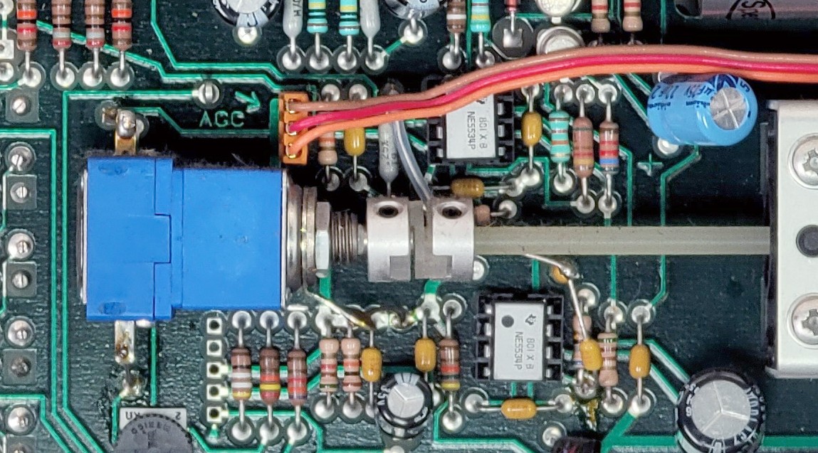
Here is that modification. I just cut a few traces and added the 1K 20-turn trimmer Manhattan style.
The new 1K trimmer R21 is used to adjust the balance of the Gate voltage. Theoretically, the optimum result is with the Gate voltage at 50% of the VDS voltage, but that is apparently not always the case.
I was expecting and hoping for a small improvement of a few dBV, but while adjusting the trimmer the 2nd H kept dropping lower and lower with every turn and eventually allowed me to drop it by a whopping amount!
Before: Overall THD 0.00021%, 2nd harmonic 0.00016%
After: Overall THD is 0.00015%, 2nd harmonic 0.000069%
That also reduces the tight specification for the two 10K0 resistors to 1%, but keeping the +/-25ppm/C.
Thanks Bob!
Using a commonly available JFET
I swapped out the original Tektronix 151-1021-00 JFET, and used the MMBF4391 instead.
After re-tuning the 2nd H distortion a bit, I now have the following results:
After: Overall THD is 0.00016%, 2nd harmonic 0.000062%.
The results are almost exactly the same so this is a good alternative.
Trying new Opamps
I've ordered a few of the OPA1655DR Opamps, to replace the three NE55534 Opamps in the generator, and the one in the output amplifier.
All the measurements I'm showing so far are straight from the generator to a 600 Ohm -10dB attenuator and then to the E-MU 0202, bypassing the output amp.
I installed the three OPA1655 Opamps in the generator and made a new measurement.
These "super" Opamps did not bring the anticipated or hoped for results.
THD went from 0.00016% to 0.00018%, a little higher
2ndH from 0.000062% to 0.000047% , a decent improvement
3rdH from 0.00012% to 0.00016%, a little bit higher
It seems that these more modern but also much more expensive Opamps are not worth it. Several people have tried a list of other Opamps with similar disappointing results. On the other hand, it also shows what an excellent result was obtained by carefully crafting the circuitry around the old but venerable NE5534's by the original SG505 design team.
I will leave the OPA1655 in place for now, but for the next revision PCB, I will switch back to using the NE5534.
New Output Amp Opamp
Now that the OPA1655's arrived, I soldered one on a DIL carrier to try it in the output Amp and see if it makes a difference there.
For reference, here is amplifier with the NE5534 result and the already tuned 2ndH:
THD is 0.039%, 2H is 0.032%, 3H is 0.021%, 4H is 0.0066% and H5 is 0.00098%.
What is interesting is that the 2ndH trimming does nothing. It shows that the 2ndH created by the output amp is dominant.
So here is the output amplifier with the OPA1655, after trimming the 2ndH (that works again):
A rather dramatic improvement I think.
THD is now 0,0014%, 2ndH is 0.00059% and 3rdH is 0,00038%, 4thH is 0.00056% and 5thH is 0.00018%. This is getting much closer to just the generator output, and is very promising.
Mind you, this is still the protoboard build with only a socket for a THT JFET, so I hope to be able to wring some more performance out of this circuit when it's on a proper PCB layout with ground planes and a way to test a few other SMD JFET's.
After an hour worth of warm-up time, I could re-adjust the 2ndH further down again, with even better values:
THD is now 0,0012%, 2ndH is 0.00013% and 3rdH is 0,00033%, 4thH is 0.00056% and 5thH is 0.00018%.
With this result, I can now go ahead and add the output amplifier section to the main board.
With all this, I've also arrived at a point where most of the challenges are fixed or understood, such that I can now move forward with the completion of the project, and produce a fully functioning and complete instrument.
That process is described here:
https://www.paulvdiyblogs.net/2025/08/diy-rebuild-of-tek-sg505-instrument.html
A Github repository is available here that has the latest information. Do not use the data in this Blog because things have further developed.