This will be a description of my process to build an AC/DC Dynamic Load.
Below is the latest version of the prototype, shown here so it will feature on the Blog post summary.

Why am I motivated to embark on this project?
I already have a Dynamic Load, described here (https://www.paulvdiyblogs.net/2015/08/dynamic-dc-power-load.html). This instrument still serves me well while testing Power Supplies and applying loads to DC outputs. It is a rather simple analog Constant Current Dynamic Load, but also has a pulsed output possibility and an offset capability so you can set the minimum and maximum current while pulsing.
For a new Dynamic Load, I initially wanted to add more modes like Constant Voltage, Constant Power (wattage), Constant Resistance and a Battery Discharge option. This means that it will have to be a digitally controlled instrument.
There are many designs that accomplish this already, but I could only find a single one that implemented an AC input, next to the usual DC input. The AC capability is useful for applying a load to non-DC inputs, like an AC sinewave coming from transformers so you can profile them, and also other waveforms like triangle or pulsed like PWM signals.
Another major reason to do this project is because I'm curious to see what is involved with AC measurements. (turned out that I had my work cut out because it's a lot more complex than I anticipated)
The initial challenges
The first challenge is to see if I can combine a DC input with an AC input. Adding an AC input requires a rectifying bridge so we can still use a MOSFET to create the load.
Adding AC inputs will also go hand-in-hand with a True RMS measurement capability which is an additional challenge for me. (it was indeed!)
To top this off, I also wanted to use the new Raspberry Pi Pico board. It has a lot of interesting features and also has a dual core. This may be required to calculate the True RMS voltages if I decide to do that in software. Dedicated chips that can do that are pretty expensive.
The initial Specifications
I have not decided on a set of specifications yet. My initial requirements for the design phase will be if I can get up to 400VAC (Vpeak) at say 200mA. The only reason I want to have a 400Vp capability is that I missed that during the designs of the VBA Curve Tracer. A more used lower voltage could be 60-80V at 1-2A to test 56Vrms transformers that I have and the most used range is up to 30Vrms at 3-5A. I hope that about 150W will be sufficient and rather easy to deal with thermally speaking. I don't need a larger current sink, these specifications should do for my own use.
The unit should have a "pulsed" mode to test transients, and as I mentioned above, a battery discharge feature. I'm not interested to build a Windows/PC controlled unit, that's beyond my capabilities, but I could possibly create an interface that is compatible with existing PC-controlled software applications.
The user interface itself will be very simple. I envision a rotary encoder for the settings and menus, with maybe only one or two toggle switches or push-buttons for power and to switch the load to the DUT on and off. I will try to use the rotary encoder push button to enter values and select menus. No key-pad! The display will most likely be a small 128x128 OLED display, most likely in color because the price difference between color and monochrome is very small these days, maybe a touch-version.
The enclosure should be as small as possible, because the available real-estate in my lab is very minimal. So there you have it. Most of it will be clarified or solved during the design phase.
Standing on the shoulders of others
I have been collecting various designs from others and looked at the way they did things. Several stand out, like the multi-part Youtube series from John Sculley:
https://www.youtube.com/playlist?list=PLUMG8JNssPPzbr4LydbTcBrhoPlemu5Dt
Unfortunately, John is no longer posting and I fear that he may no longer be with us. He will be missed by a lot of enthousiasts, like me, that thouroughly enjoyed the many projects he created, and the excellent way of presenting them.
Recently, I discovered a vastly improved version based on the above project. It has significantly improved hardware and has really excellent software.
https://github.com/Dominik-Workshop/Electronic_load/tree/master
Then there are the contributions from Jay_Diddy_B on the EEVBLOG.
https://www.eevblog.com/forum/projects/dynamic-electronic-load-project/
I also studied the tear-down and schematics of the Array 37XX Dynamic loads done by another frequent user, Kerry Wong, that can be found here:
http://www.kerrywong.com/2018/11/05/teardown-of-an-array-3711a-300w-dc-electronic-load/
Here is another one:
https://www.instructables.com/Arduino-Programmable-Constant-Current-Power-Resist/
As I mentioned earlier, I could only find a single DIY design that features a true AC/DC capability. That project from Rainer Schuster is relatively current (published on November 2019) and can be found here:
https://www.elektormagazine.com/labs/electronic-load-for-dc-and-ac (there are two versions of diagrams available, you really have to search for the latest one)
Here is a YouTube video of the instrument with an elaborate explanation of the AC mode of operation and background theory.
https://www.youtube.com/watch?v=YXUa-xOSNLE
This project will be my reference model.
My Humble Beginnings
To start with the project, I build a minimal load circuit, with just one Opamp and one MOSFET. This allows me to study the parameters, and add more functionality as I go.
Here is the schematic diagram I'm starting with:

And here are pictures of the hardware contraption:

The power connections to the MOSFET need to be as short as possible, so I mounted the current shunt, the anti-oscillation capacitor and the rectifier bridge right on the MOSFET or close to it.

The rest of the parts are not that critical at this point.
I used my precision Siglent SPD3303X-E DC Lab supply (1mV/1mA resolution) to act as a DUT, and I set channel 1 to supply 10V at 2A. It allows me to monitor the current into the load. Channel 2 was used to supply the reference voltage going to the positive input of the Opamp. I used a second simple DIY lab supply to supply the +/- 12V rails for the Opamp.
My Siglent SDM3065X DMM was used to measure the Gate voltage (VGS) while adjusting the CH2 reference voltage that will regulate the current into the load.
Because I use a 0.1 Ohm current shunt, the relationship between the reference voltage, supplied by the Lab supply, was 10mV in to get a 100mA load current. I used my Lab supply's display to verify the supplied current. Setting the reference voltage to 0V produced a current of 2mA. That tolerance value can be adjusted in the final circuit with the Opamp nulling. Increasing the reference voltage with 10mV increments showed the current to stay in-step all the way up to 2A, which I set as the maximum for this test setup.
I then used my FeelElec FY6900 Function Generator to supply a DC pulse instead of the reference voltage. I selected 100Hz as the frequency, a duty cycle with 30% on and set the pulse with an offset of 10mV and a maximum voltage of 40mV. This resulted in a load current fluctuating between 100mA and ( 10+40) 500mA. I used my Rigol DS2072A (modified to be a DS2302 300MHz) DSO to look at the Gate of the MOSFET to see the effect, and a second channel to monitor the Source. I then increased the frequency to 1 KHz and all was well. With this prototype contraption, it makes no sense to go further to try higher frequencies. I also increased the maximum pulse voltage to get a current switching from 100mA to 1.5A without any issues.
I then profiled the VGS to IDS relationship, to see how much of a rail voltage I need for the Opamp. It turns out that the MOSFET is off at a VGS of 3.08V and needs 4V to let a current of 2A through. Some more measurements are in the schematic. This means that I probably only need about +8V for the positive supply of the Opamp, and I also only need -1 or -2V for the negative supply to really turn the MOSFET off under all conditions, mostly when I pulse it.
What the effects of the minimum rail voltages will be with non-DC loads I don't know yet, that's something I will be able to test soon, because I need an analog multiplier (AD633) to do that. The multiplier is needed to "marry" the AC DUT waveform with the Gate voltage to make the current follow the voltage of the waveform.
Selecting the final rail values depends on the rest of the design.
Initially, I used the NPN/PNP Gate driver circuit that was in the original schematic Rainer uses, but decided to take it out for now. It's not needed at this moment. The On-Semi FCH072N60 MOSFET I use has a Ciss of 5690pF vs 4200pF for the SPW32N50C3 in the original design that can handle 560V at 32A. The one I use was tested in our Curve Tracer project. It is a 600V 52A device where the SOA diagram shows it can still handle 1A at 400V. We'll see about that later.

I also have two IXOS IXTH 80N075L2 linear MOSFETS, they only go to 75V and I should be able to get 4A at 50V out of one. I've never used a linear MOSFET so this is another learning experience.
The part's arrived, and I wanted to add the AD633 multiplier to my bread board. I ordered the SMD version so I soldered it on a carrier and used Rainer's original schematic to wire it up. Seemed simple enough, but when I tried it, it didn't work. There was a 25mA current flowing from the negative supply, oops!
After trying a few things, I took it out of circuit and built a little test circuit just to test and verify the AD633. No dice, I was afraid that I could have blown the part by statics, something that's very rare for me. After a while tinkering some more I decided to study the specifications in more detail, and then it dawned on me. The pin-out for the PDIP-8 version, that Rainer used, is very different from the SOIC-8 that I have! I don't remember to ever have encountered such a difference in pin-out between packages.

I probably damaged or destroyed the part by forcing -12V into the output amplifier (pin 5), which is a real bummer, because these things are not cheap. Analog Devices calls them "modestly priced packages", but with pricing close to $20, that's not modest enough for me.
I studied discrete multipliers to see if I could use them as an alternative. Unfortunately, I couldn't get LTspice to get a decent and reliable output out of a few different circuits I tried, so I gave up on that idea and ordered a new AD633. This time from a supplier that has the PDIP version, so I can more easily use it on my breadboard, and use a socket on the final PCB layout. It will take a few days to get here.
Unfortunately, the chip that arrived does not work either. The output does not follow the inputs and is always at a fix level of about 5V, even with grounded inputs. Building the Fig. 13 circuit in the datasheet shows no frequency doubling and only distorted waveforms. This chip came from a reputable supplier and I reported the issue to them. I also ordered a third chip from a supplier in France through eBay that will get here in 1-2 weeks.
Update: The supplier was so kind to send me a replacement chip. The other one I ordered is in the mail. This is becoming an expensive chip for me...
I got the replacement AD633 and it seems to work in my test setup. Finally! More on this later.
I got the other chip from France, ordered from eBay today and checked it out...not working at all! This was almost to be expected, I've reported it and asked for a refund and eventually I got my money back.
Using the good AD633JN chip, I expanded the earlier test circuit to include it.

The analog multiplier is fed with the "rectified" DUT voltage at the X1 input, and the Y1 input is connected to the V-ref supply. The DUT supply is reduced 10x by a resistor divider and the X1 input is also protected by a 10V Zener. In order to get a linear relation between the V-ref and the DUT current, I found that I needed to use a trimmer (RV1) to calibrate the 1:1 current/voltage relationship. Note also that because of the internal divide by 10 operation of the AD633 multiplier, the V-ref now needs to be 10x larger, so now a 100mV input results in a 100mA DUT current.
Another trimmer (RV2) is used to calibrate the DUT current to zero with no V-ref input. This needs to be calibrated first, and then the DUT voltage trimmer.
At this moment, I'm still using a DC lab supply for the DUT. The DC supply voltage is adjusted such that I have 10.00V at the Source of the MOSFET, compensating for the voltage drop over the bridge. This allows me to calibrate the X1 input to 1.00V resulting in a linear V-ref to DUT current at 10V. By using the Lab supply, I can also monitor the DUT current.
Note:
Due to the internal multiplication of the AD633, raising the DUT voltage from say 10 to 20V also doubles the DUT current because W=(X1*Y1)/10. This is a major departure from the normal DC load functionality for a CC mode, because the voltage should be independent of the set current. (hence CC).
As a minimum, the display should show the correct volts and amps, so the microcontroller needs to use the DUT voltage to adjust the current reading correctly, or adjust the V-ref level to keep the current constant (CC) so the Wattage will be the same.
Using a sinewave as the input
Switching to an AC input, I used a center-tapped 12-0-12VAC transformer with an E-I laminated core as a DUT supply. My mains has 50 Hz. Let me show you what I'm seeing using only one 12V tap.
Here is the AC signal from the transformer. Note that it's not a perfect sinewave, but for a transformer, this is quite normal. The flat tops are most likely due to the metal core saturation. Note the bottom readouts of the DSO. Vpp shows a value of 42.4V, although this is rated as a 12VAC transformer. The transformer specification is actually in Vrms and is a cause for confusion, which is the same as for mains voltages. A 230V mains is only the average, so be aware that the peak voltages can be a lot higher.
Next to the more used and familiar Vpp, I'm also introducing the Vrms voltage on the DSO so we can keep track. To avoid DC offset and different waveform mistakes by the Vrms calculation, it is best to always switch the DSO input channel to AC coupled to measure Vrms correctly.
The transformer delivers 14.47Vrms according to the DSO, and to verify this, I used my DMM. It measures 14.61VAC, which is close enough. This level is OK for a 12Vrms unloaded transformer.
It has been reported that a DSO can actually measure the Vrms waveform very well, because it could use every stored sample of the waveform and calculate the correct Vrms value based on the many stored samples. (see my additional post about a software based rms calculation below in the supporting section below) If my Rigol really calculates every sample I don't know. Note that for a valid calculation, the waveform should fit the screen and should have at least one full cycle and little noise.
Note that the above screen capture does not have a complete cycle!
Here is another sample, but now with a higher horizontal setting of 5ms to show more complete cycles.
Note that the Vpp stays the same, but the Vrms went up to 14.93. This can be a real trap if you don't know your instrument well enough. (I didn't...) So be aware!
The on-line calculator on the Web shows a value of 14.99Vrms, which is close enough because it's not a perfect sinewave.
For the next screen shot, CH1 is measuring the voltage after the bridge and CH2 measures across the current shunt of 0.1 Ohm. I used a Vref setting of 500mA.

The bridge rectifies both halves of the sinewave, resulting in the "flipped" negative side into a positive voltage. That's perfectly normal, but I'm showing it here in detail so it is clear for everybody.
As we see, the current closely follows the voltage, which is what we want and it shows that the AD633 is doing it's job.
The Vpp value of the double rectified signal is now about halved to 19Vpp. The input sinewave was 42.40Vpp so it should be 21.20Vpp. If we assume a voltage drop of the two diodes in the bridge of 0.7V each, we still have a loss of 21.2 - 2*0.7 = 19.8 - 19.0Vpp = 0.8V so we miss another 0.8V somewhere, probably due to the flat bottom section of the double rectified waveform.
The voltage across the 0.1 Ohm shunt is 26.4mVpp or 6.912mVrms. The real current should be 26.4mV x 10 because of the 0.1 Ohm shunt = 264mV. The DC equivalent voltage is twice the average, so 528mV, while we set the load for 500mV. Pretty close but not precise.
There are a few issues we need to address. Where is the 0.8V extra loss coming from, and why do we have different voltage levels. Granted, the waveforms are not really textbook pure, so that may explain some of it. Furthermore, can we figure out where the difference in set and real current comes from?
Let's see if we can figure this out.
First of all, the Crest factor for the full sinewave and the double rectified one is exactly the same. This is used in the rms calculation, so should not matter. See the table below. This could point to the poor waveforms so here's another gotcha to watch out for.

Let's see if we can verify the waveform purity issue by using an FG and create the same situation, but now using a close to perfect (albeit digitally created) waveforms.


Also a far cry from the textbook waveform above! The DSO shows 3.00Vpp and 1.012Vrms. The DMM shows 1.004V. The calculated Vrms from 3.0Vpp is 1.060V so that is close enough.
Note that there is an imbalance in the waveform, probably because the diodes I used are not matched. Could also be mains induced hum.
Here it becomes interesting. Let's do the same calculation as we did with the transformer. You would assume that the input voltage to the bridge of 8.8Vpp would be halved to 4.4Vpp, but it is 3Vpp, a difference of 1.4V. We know there is a voltage drop of two diodes in the full bridge, so the drop must be approx. 0.7V per diode. That seems plausible, so this time, we don't have an additional loss.
However, this time we have virtually no current flowing through this bridge and we had about 0.5Amps with the transformer. Could that explain the extra loss? We know that the voltage drop of a diode increases with a higher current, so at least partially, that could be it. We may now have a plausible explanation for the majority of the 0.8V extra loss.
Now back to the set vs measured Vrms value for the voltage across the shunt. In the DC mode, and with a Vref of 500mV and a 10VDC input, we calibrated the system to deliver a 500mA DUT current.
With a sinewave, the DSO calculates a Vrms of 26.4mV over the 0.1 Ohm shunt so that should represent an rms current (Irms) of 264mA. This is not with a 10VDC input voltage but with an AC of 12.4Vrms. If we assume that the current is an average for the waveform, we could double the measured current to get back to the set current. That would mean a measured 528 versus a set 500mA. Could that be it?
Keep in mind that the AD633 does not deal with rms values! One input of the chip gets a DC signal (Vref) and the other input is getting values that are represented by the CH1 yellow waveform we see on the DSO, so peak-to-peak values of a double rectified sinewave and they get multiplied together by the chip to drive the MOSFET that also sees the full bridge rectified signal.
Like the AD633, we would need to make calculations all along the current waveform to see if they are indeed correct.
I tried a few methods to calibrate the Vref input levels 1:1 to the current outputs. I did not really succeed because the linearity is not that precise. Here is what I mean:


Unlike precise and stable DC signals, I'm afraid that with AC waveforms, the instrument may never be precise. This seems to be a function of the crest factor (how pure is the sinewave) and how much is the voltage deviating with higher currents, which will influence the multiplication. Also we have to assume that the multiplication of the chip itself may not be perfect and not 100% linear.
Using a triangle as the input
To test another kind of waveform, a triangle, I used the DUT supply from my Curve Tracer (described in another blog post). Applying 24Vp-p and using a load of 500mA produced the following display:

The current waveform is nicely following the DUT voltage, with some aberrations at the null transition. The flat bottoms of the triangle is caused by the bridge diodes. CH1 (yellow) is measuring after the bridge. CH2 (blue) is measuring across the shunt. The load was set at 500mA.
This looks OK, but is still not very precise.
Profiling a transformer
One of the applications I had in mind for the AC/DC load, was to profile transformers. I once took a transformer out of a printer, but it had no markings. I ended-up using power resistors to figure out where the serious voltage droop level was and used those numbers.
The transformer I used for the first measurement is a center tapped 12-0-12VAC transformer, rated at 2A. To check that, I connected one of the 12VAC windings to the dynamic load and turned-up the current until the transformer could no longer output 12VAC, and the voltage dropped off rapidly. I used one DMM to measure the transformer AC output, and looked at the DSO for more clues.
The DSO reported 14.29Vrms for the transformer output, while the Fluke 76 showed 14.68VAC. That's close enough.
The good news was that I could turn up the Vref voltage to 2.2V = 2.2A before the AC voltage dropped below 12V. The Fluke reported that happening with a current of 1.98A, which is the specification for the transformer. This seems to prove the value of this instrument.
This is what the DSO shows:.
I guess this begs the question how good we can make this particular measurement without using the two DMM's, and use the Arduino and ADC's to measure and report the DUT RMS voltages and current.
That task will be addressed next...
Preliminary conclusion
My original plan was to build one instrument that could measure Constant Current (CC), Constant Power (CP) and Constant Resistance (CR) for AC and DC inputs and also have a DC battery discharge option.
A simple dynamic CC mode can be constructed without a controller in the loop. This is how I build my current Dynamic Load, as a matter of fact, is has no controller at all. The hardware circuit does it all, and an optional controller can be used to display voltages and currents and set the values. The disadvantage of this approach is that the current you set is only valid for one DUT voltage. If the DUT voltage changes, the current will no longer be what you set it at. This can also be done for AC voltages.
For true dynamic CC, CP and CR modes, you -have- to use special hardware or a controller to actively control the current for the MOSFET, based on calculations that include the DUT voltage and the current. Doing this also for AC voltages is a challenge.
After making the above measurements and analyzing them, I came to the conclusion that my current approach of using one instrument that can do both AC and DC inputs is too much to ask for in a simple system. The mere fact that we need a multiplier in the circuit for AC signals, defeats the "constant" factor in all the measurement modes. As with a true dynamic instrument, the microcontroller continuously needs to measure the input voltage and re-calculate the current setting to keep the set current value, to create true CC, CP and CR functionality. This requires a tight loop for the controller that for AC rms calculations will really task the processor with all the other tasks, like displaying the measured values on a display.
The simple solution is to just let the current change when the DUT voltage changes but in that case it is no longer in a true dynamic CC mode, and the DUT current may no longer reflect the set current.
So my conclusion at this moment is that it will be really hard to marry AC and DC input values with the same hardware. Everything will have to be under very tight real-time control by the CPU.
So what are the options?
1. Build a simple AC/DC load
You can build a simple instrument for AC and DC signals only that is probably limited to a pseudo real-time CC mode with limited measurement precision. As we've seen already, it can be used to profile transformers and the likes. To keep it simple, there will be no real CC load, just a load you set that is true for a certain DUT voltage. If the voltage changes, you have to re-adjust the current. This will have limited precision, but will function as a load.
2. Build a full fledged DC load with high precision
This is a dedicated DC only instrument that can be fitted with all the required modes and that can have a very high precision. This has been done many times already by others and is less of a challenge for me.
3. Build a combined AC/DC load with CC, CR, CP modes
If you want to have real (true) CC, CR and CP modes for AC and DC, this will be a compromise due to the loss of precision, unless this can be fixed somehow in software. It also needs a very fast and tight control of the current while taking the DUT voltage changes into account. I'm suspecting that could be beyond the capabilities of a simple controler like an Arduino Nano.
4. Use a relay to switch from a DC to an AC input
A lot of the troubles I encountered was based on my decision to use the bridge for AC and DC signals at the same time. This can be done, but than you have to take account of the bridge diode characteristics (the voltage drop), that changes with different currents. Rainer used an AC/DC mode relay for his design, maybe I need to do that too.
Having said all that, I need to rethink my goals and for now I will continue with the development of the combined AC/DC signal input, but first try the capabilities of software RMS measurements and see how far I can get.
This means that we have to now start with the voltage and current measuring by an Arduino Nano, to keep things simple.

I found two libraries for the ADS1115 that I tried, but settled on the Adafruit version.
I also figured out why I blew the ADS1115 chip. The prototype that I had put together had the -12V and the GND rails on the top side of the breadboard, and when I wanted to ground one of the ADC inputs, I must have touched the -12V rail, blowing the input protection diodes of the device and then taking the rest of the chip with it.
Overall, the prototype was getting unwieldy by now and with so many connections I was having problems. Now that most of the circuits were sorted out, I soldered everything on a proto-board, using sockets for the chips.
I also put together a small and rough test sketch together for the Nano such that I can now display the DUT voltage and the DUT current on the LCD display. Right now I only display DC voltages and currents.

This is as far as I got today, I'm pretty happy with the results.
Now that I'm satisfied with this setup and sketch, I'll turn my attention to converting the rms measurements. I expect that will be a challenge (it was!). I've got a pretty good idea now how to convert a voltage to RMS (not!), but need to pick a method out of the several that I found, and then see if I can implement it on the Nano.
Unfortunately, I ran into an issue with the ADS1115 that stopped me from going forward. Have a look below at the topic called: "Calculating the RMS value of a waveform" for details and a solution. In a nutshell, I discovered that the serial communication with the ADS1115 is way too slow to be used with rms calculations. The rms calculation requires that you measure a 50Hz cycle at least 40 times to get reasonable precise rms values. That's way too fast for serial interface based ADC's.
So with the RMS calculation topic more or less solved and understood, I can now start to use it with the prototype hardware. First of all, I needed to eliminate the AD1115 out of the circuit and replace it with the on-board Nano ADC's and live with the reduced resolution back to 8-bits.
After a lot of struggles, see the RMS and ADC topics below, the prototype hardware is now working with the on-board ADC's from the Nano, and are producing results for the DUT voltages and the voltage across the shunt.
Another misunderstanding
What I still don't understand is the difference in voltages measured before and after a dual rectified bridge. With my DSO, I measure 40.8Vpp before the bridge and 18.4Vpp after, and not, as I expected 50% of 40.8 = 20.4Vpp, a difference of 2Vpp.
This drop seems to be caused by the bridge two diode drops, but without a load, is should not be more than 600mV each so 1.2V. It's close but where is the remaining 800mV?
When you measure Vrms however, it's also not half, but different. The same 40.8Vpp is measured by my DSO as 14.71Vrms. My DMM measures 14.51Vrms which is close enough. When I put in 40.8Vpp in the online calculator, it shows that I should have 14,4249Vrms. That's all close enough.
However, on the other side of the bridge, the DSO now measures 18.4Vpp and 6.7Vrms. My DMM shows 6.44Vrms. They are relatively close, also because the numbers fluctuate a bit. The online calculator shows that I should measure 6,5053Vrms, again close enough, although the online calculator assumes a pure sinewave. Because the Crest factor is the same for both waveforms, it works and that was the foundation for my attempts to measure after the bridge but show the value from before.
But, why is the voltage after the bridge not exactly half the Vrms value from before the bridge? If I use the online calculator, half of the 14.4249Vrms before should be 7.2123Vrms after, but we measure a loss of 707mV, which seems to indicate only one diode voltage drop, not two. Why?
Again, I want to measure the DUT voltage after the bridge (measuring DC is easier), but show the value from before the bridge. This makes the circuit easier and without potential grounding issues, and use much higher Vpp values to deal with. Unfortunately, this discrepancy means that I will have to use fudge factors to get it about right.
Rainer used a a relais to switch from the AC mode to the DC mode and thereby avoided all the above troubles. Maybe I should declare defeat and follow his lead.
For now, I used my DMM to calculate the conversion fudge factor and added that to the script. Unfortunately, it's OK but not very linear with different input voltages.
Vrms readings fluctuate a lot
What I also found is that the Vrms measurements fluctuate and are certainly not useful at all with 3 decimal digits. My DSO and also my highly accurate DMM also show these fluctuating values, so two digits are more than enough and that gives me room to display the rms suffix. I also need to add Opamp buffers for the two ADC inputs to reduce the noise and take care of the Nano capacity switching at the front of the Mux.

It's also becoming clear to me that with this setup, I don't need a very precise DAC anymore. I think I can manage by using the Nano's PWM feature and create a poor-mans DAC. I'll try that soon.

Latest schematics:


The sliding switch on the left edge is the AC/DC mode switch for the software.
A heads-up for a potential risk
Let me add a word of caution at this stage of the design.
When you are going to connect the Dynamic Load circuitry to a real DUT, especially one with higher voltages, and also connect a USB cable between the Arduino Nano on the DL and your PC, you run a big risk!
The GND of the Dynamic Load circuit will be connected to the DUT GND or one side of the AC connections, and through the USB cable, also to your PC. Depending on what your DUT is, and what the ground potential is, it is entirely possible to blow-up your PC or as a minimum the USB interface if it's earth ground connected.
I strongly recommend you to use an optically isolated USB connector interface in-between the Arduino Nano used in the DL and your PC.
Don't risk it, use an optically isolated adapter, they are a lot les expensive than a new PC. Here is one from Adafruit, it sells for $35 but you can get less expensive ones as well. Amazon sells one for $15. I got myself an even cheaper one from Aliexpress because the USB transfer speed is less important for this application.

Understanding the reported values

Input attenuation circuit

Here I have added the schematic with the 400V/100V input attenuation and the selection jumper and that's what I now have in the prototype as well.
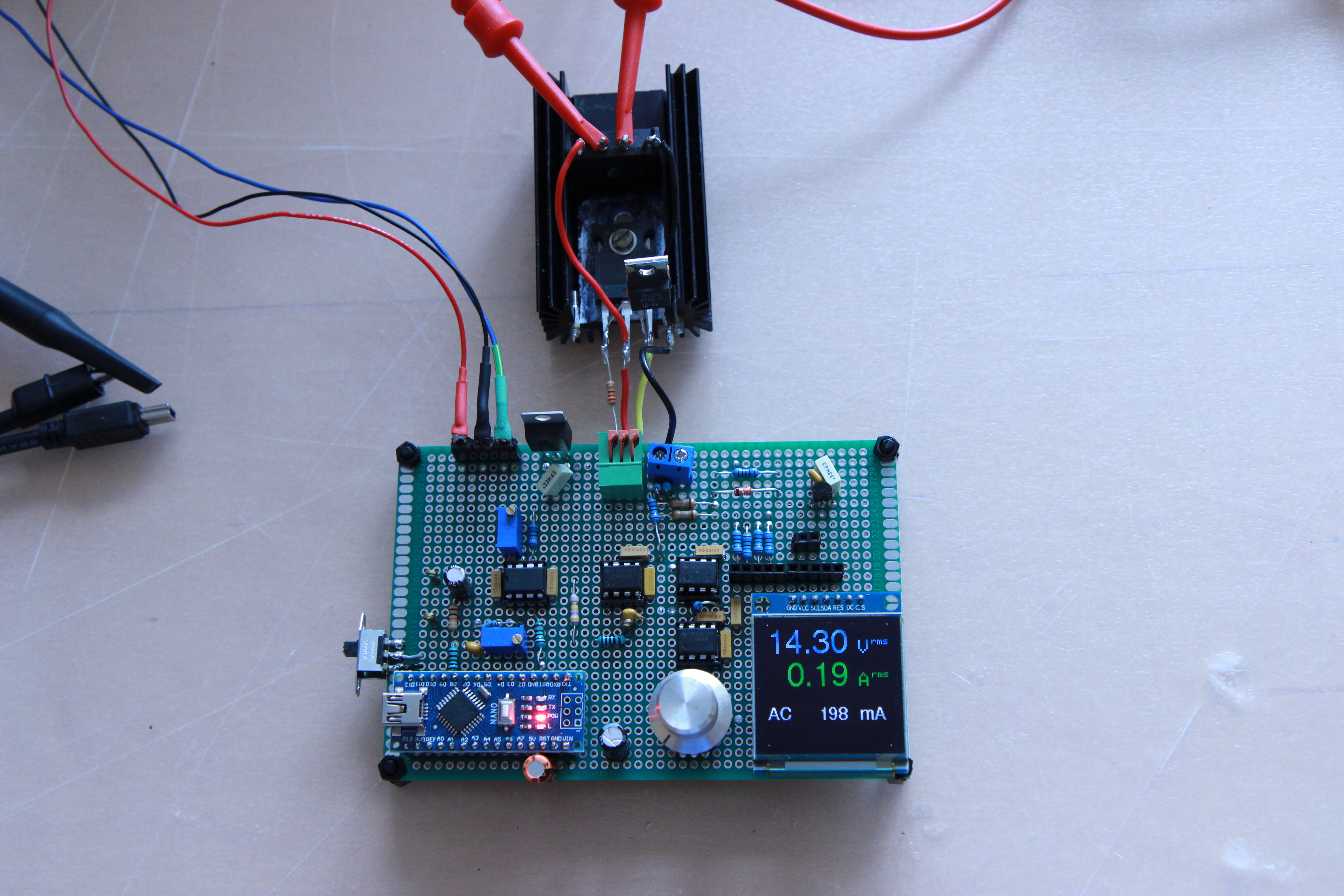
Here is the latest version of the prototype:

Compared to the earlier picture above, in the top left is the carrier with the LTC1966, above it is the TO-92 -5V regulator. In the same row, to the right of the blue trimmer is the Opamp used for the protection of the LTC1966 input signal. Top right has the jumpers for the h/w or s/w RMS calculation setting, and the jumper for the input attenuator that now selects between 400V and 100V.
On the display you see the measured RMS voltage, calculated so it's reflecting the input to the bridge, and the resulting DUT current. The last line in white shows that the mode is AC and the current setting by the rotary switch is set to 200mA.
[Time-out period]
I became more and more frustrated and unhappy about the poor measurement result precision and the weird fudge factors I had to use, so I decided to take a break from this project and put it on ice for a while, while I worked on other projects that needed my full attention.[UPDATE Dec 2023]
While I worked on a few other projects, I could not leave this one unfinished. After spending some more time with Google, I got some ideas for a possible solution for the pesky problem I have described earlier to reliably and accurately measure the AC voltage at the DUT side.
The True rms to DC convertor, the LTC1966 I use at this moment, is fed with the already rectified voltage after the main bridge, in an attempt to measure on the "right side" of the load that feeds the Arduino. In principle, this is perfectly OK, because the Crest factor for a sinewave and a double rectified sinewave is the same. I am also currently using the single-ended input mode for the device. The trouble is with the weird voltage measurement results before and after the bridge, requiring fudge factors that are not linear.
After looking at other circuits and re-reading the LTC1966 datasheet I was hoping that by using the differential input mode of the LTC I would avoid the grounding and therefore the bridge issues. This would remove some of the fudge factors I had to use to get the same readings as with my DMM. This is caused by the voltage drop over the diodes in the bridge, unfortunately, as we already know, this voltage drop value also changes with the current.
I looked at two other methods to address the bridge issues, and first considered using Schottky diodes for the bridge because they have a lower voltage drop. Unfortunately, these diodes are not available for higher voltages and currents. Another seemingly perfect solution I looked at is that of an ideal diode bridge using MOSFET's.
The rather extensive testing of this type of bridge turned out to also have too many limitations, so I dropped it. The details of my findings can be found in the supporting section below.
The DUT current vs voltage issue
As I reported earlier, the working of the AD633 multiplier causes the DUT current to change based on changing DUT voltages. As an example, when you set the DUT current to say 100mA and the DUT voltage is 10V, the reported voltage and measured current match the set current.
However, when you double the input voltage to 20V, the set current will stay at 100mA, but the real DUT current will double to 200mA (Ohm's law) and the current measurement on the display shows that but not the set current, it stays at 100mA. That's the way I have designed this circuit up until now, analog to the one I already have.
The next step is to make the system truly dynamic, because we need a Constant Current mode independent of the DUT voltage and also the Constant Power and the Constant Resistor modes. This will require a different setup by which the Nano not only measures the DUT voltage and current, but dynamically calculates the current setting for the MOSFET. To do that for the AC mode can become more complicated quickly. Either way, I want to try that to see how it goes.
Adding the DUT Power (Watt) to the display
A recap of where we are now
After a lot of troubles, stumbling and falling, I have created a prototype that works pretty good, but has some significant limitations based on the choices I made. By sticking to the decision to keep the bridge in-circuit for everything, I had issues to circumvent or deal with the bridge diode drop. However, with this version, the DC modes are all gone because I find that the precision is simply not good enough. Am I barking up the wrong tree, or did I end up in a dead-end-street?
I need to think this over and find the motivation to re-start the process with a different architecture.
Differences between the AC mode and the DC mode
Here is a helicopter view of what I'm trying to accomplish and how I'm going to try to solve it.
The required use of the AD633 multiplier for the AC mode requires a different approach to the traditional Dynamic Load concept, because the DUT voltage level is included in the current setting due to the AD633 conversion (V*I/10). To counter that, I use the Nano as the software controller, meaning that the rotary encoder is used to set the desired current level but the Nano calculates the required DAC setting to drive the MOSFET based on the measured current and voltage values. This is needed such that the controlling loop keeps the desired current level to the set level at all times, even when the voltage changes.
This requires a pretty tight software controlling loop and due to the non-real time effect, the output is typically changing with about +/- 1 DAC step due to the lag in measuring the current and adjusting the DAC to compensate. This is shown and explained a little further in the post.
This method is very different from all(?) other Dynamic Load implementations where the DAC is set by the encoder for the required current and stays fixed at that setting during the measurement regardless of the DUT voltage changes due to the effect of the real-time hardware controlling loop.
The solution I'm going to implement is to fix the multiplication of the AD633 in the DC mode, So the DAC is set by the encoder for a desired current setting, and stays fixed during the measurement. When there are changes in the DUT voltage, this is countered by the hardware controlling loop.
For the AC mode, the AD633 needs to be brought back into the circuit and we need the software controlling loop.
First I'm going to see how far I can get it with the software controlling loop while still in the DC mode because that's easier, but then "take out" the multiplication factor and continue with the refinements for the DC mode. When I'm happy, I will return to the AC mode again.
Using a relays to take the bridge in and out of circuit.
I modified the front-end to have a relay that switches between AC and DC, in effect taking the bridge out of circuit for the DC mode. I replaced the SPDT switch I was already using for the software mode switching and used a DPDT version to now also switch the relays. The start-up mode is in AC, for safety reasons.
The sketch has been modified quite a lot by cleaning the structure to make it easier to work with and I combine a lot of the code for the two modes. The DC mode works pretty good now, I now need to spend a bit more time calibrating the AC mode.
Here is a quick & dirty picture of the current setup. Still need to clean the prototype up...

With these changes already made, I might as well continue and make the whole system with a dual mode, AC and DC. That means I have to revisit a number of the circuit details that actually grew on me while adding extensions and improvements.
While I was thinking about the major decision to switch the bridge out of circuit for DC inputs, and the implications, I realized that this opens a lot of possibilities again. So, I have stopped the further development of the prototype and started anew with an almost clean sheet of paper, designing version 4.
It actually means that I have to go back to the drawing board (LTspice) and rethink a number of things.
Here are the preliminary results of my activities with LTspice.

Above is the circuit that measures the DUT Voltages. It assumes the relay that will switch to the AC input mode, as it is showed above, or I can switch to the DC mode by disconnecting the output of the full bridge, and connecting V1 as the DUT DC voltage. The input divider of 500K and 70K is supplying the input for the AD633 multiplier, and is used for the 40V DUT voltage input range. The attenuated voltage is buffered by U1 and then attenuated again to provide the inputs for the Nano ADC for the DC mode, or to the LTC1966 True rms to DC convertor. I will design the prototype such that I can use the software RMS conversion, or use the LTC. If the software version works well enough it allows you to avoid this rather expensive chip. The voltage level for the LTC1966 is 1V max, and I decided to switch the Nano to the internal 1V1 reference, so it can also handle the 1V signal. It also gives me a higher bit resolution.
The 400V DUT input maximum requires the input voltage divider to change, and I do that by using R3 in parallel to R2. Initially I will use a switch or a jumper but later use a MOSFET that is controlled by the Nano. I could make that an automatic range switch by measuring the input signal and when it's higher than 1V, switch to the 400V range.
I already know that I will need two MOSFET's to handle the 4A maximum current, so I completed the design of that circuit. To create two parallel MOSFET's that share the load, you either need two completely duplicated circuits to drive the MOSFET and measure the current through the two shunt resistors. That calls for two sense resistors and two current monitors with their output summed by another Opamp.
I took another approach, one that we also used with the Curve Tracer project for the DUT supply. The rather novel idea is to have one MOSFET duplicate the current of the other one. This will solve the imbalance and thermal issues and also allows you to have only one (common) current sense resistor.
In the circuit below, the top MOSFET U2 is the main one. It is driven with the input voltage V5 to set the current. V5 will actually be the AD633 multiplier output voltage. To create a better balance between the two MOSFET's there is a 0.5R resistor in the Source. Opamp U4 monitors the current through that balance resistor of U2, and drives the second MOSFET U1, to duplicate the current through it's own 0.5R balance resistor. Both circuits are then connected to a single sense resistor, and that is used to measure the total current. I'm using two 0.5R resistors in parallel to share the current. With these values and currents, I can use 2W SMD resistors I already have.
This is the transient plot, a clean current switching with 10ms pulses, no under or overshoot. The current of 2A you see is produced by one of the two MOSFET circuits and should be doubled for the total.
You will have noticed that I added the transistor totem pole drivers for the Gate's back in. Because we will be driving the MOSFET's with AC signals, we need to remove the Gate capacitance quickly and will need that higher current drive capability to do so.
Another Opamp is measuring the voltage across the sense resistor and feeds that voltage to the Nano ADC so we can record the current. That voltage is 1V with a 4A load.
A 1V input to the current setting circuit will result in a 4A current through the DUT.
I have added two Gate clamping resistors of 10K to GND because I discovered that with my prototype with the overall supply voltage accidentally removed, the MOSFET's were wide open and things got hot. You want to avoid that situation from happening. It also solves a start-up glitch I was noticing with LTspice. These resistors also help with the driving of the Gates.
The FCH76N60 MOSFET's that I'm using in LTspice is a placeholder for the FCH72N60 that I'm actually using. I cannot find a model for that version, but the specifications are very close. The 76 part seems to be more modern.
Below are the schematic diagrams that I will be working with now. I did not update the capacitor changes yet that resulted from the LTspice analysis, the rest is OK.
I've added a relay that can be used to disconnect the DUT from the circuit. This is so I can test the effects of disconnecting the DUT from the system, and see the effects of the MOSFET regulation. Just connecting/disconnecting the DUT can be harmful for both because the MOSFET's can be driven to fully open when there is no DUT. Connecting it again will result in a huge current spike. I need to add protection, and can test that with this setup. In the "final" version, the Gate of the MOSFET's will be forced low somehow to stop them from conducting. Also, we need to have some protection for very low DUT voltages, because the current/wattage can get out of hand quickly. I hope to fix all that with this prototype.


Here is the 3D view of the PCB:

The elaborate cut-outs at the front are designed so it fits my heat sink.


The cut-outs for the PCB will fit the two MOSFET's, the LM35 temperature sensor, and the diode bridge. In the little area in-between the ribs, I located the mains input connector and the fuse. I will use wires to connect the mains signals directly to the transformer on the bottom of the PCB. I don't want them routed on my PCB.
There is a complicated looking keep-out area for the ground-plane where the 400V of the DUT are routed on the board. Also the MOSFET's do not have a ground plane near them. I now use three resistors in series for the attenuator for the up to 400V DUT signal, to provide a more than sufficient spark-gap.
The whole contraption will go in an enclosure that looks the the one I already use for my current Dynamic Load. A 15x60x60mm 12V fan will be mounted on top of the heat-sink, like I also have with the Dynamic Load. It's also the same enclosure that I used for my own designed Power Supplies, that I no longer use.

While waiting for the PCB I will make some changes to the current prototype and see how close I can get to the above schematic and do some more tests. I will also work on the software side of things.
The focus now is to work on the DC side of things, and later work some more on the AC capabilities.
I now have the Constant Current, the Constant Power and the Constant Resistance modes working with the current prototype. Pressing the rotary switch button now cycles through the CC, CP and CR modes and updates all the suffixes. This works really nice now, and the system is very responsive with a loop-time of 1.8mS.
I need to do some more measurements to see how well the CC, CP and CR modes really are working for the DUT. I may have to wait for the new prototype, we'll see.
I did not calibrate any of the measurements yet, so that's not in the code on the Github. That will have to wait until I get the new prototype because that will change things quite a bit.
The V4 prototype
Here is a picture of the assembled PCB. I tested the rails and had to fix some soldering issues, but that's all done. Now for the main part, but first adopting the sketch to this version of the hardware.

I had to fix a few hardware errors that I made, they are fixed in the schematics above. I also had the make several changes and additions to the sketch. It's coming together, albeit very slowly.
Software controlling loop fluctuation problem
After getting the prototype up and running and playing a bit with it, I discovered that my method to regulate the CC-mode in software has a major draw-back. The controlling loop is fluctuating around the requested current setting.

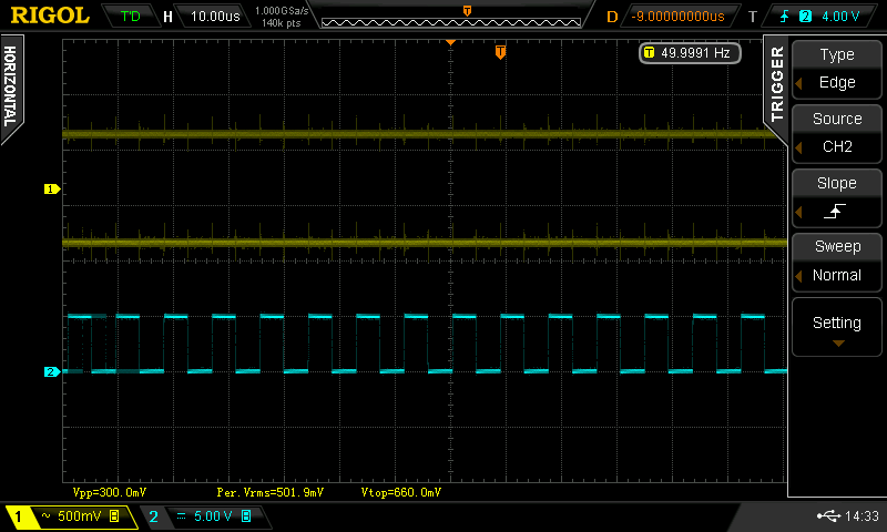
Channel 1 (yellow) is the Gate voltage of the main MOSFET. This voltage is the result of the PWM output (DAC) that fluctuates somewhere between a count of 20 and 79.
The Gate voltage is a function of the controlling loop duration during which the DAC is driven by the compare of the current setting of 200mA in this case and the actual DUT current by measuring the shunt voltage. The other contributing factor is the multiplication of the DAC output times the measured DUT voltage by the AD633. I was hoping to get a result of the DAC counter +/- 1, but alas, it is a lot worse.
The pulse train in blue above shows the approx. 1.8ms loop duration of the sketch. The gap of about 80-100ms in these updates is caused by the blocking event of the SPI communication to the OLED display which happens every 500ms.
The SPI blocking is not the main cause, but contributes to the "instability" problem, because during this period, there is a gap in the tracking.
Here is a picture that shows the root cause of the problem:

The current is set by the decoder at position 20, and that multiplies by 10mA/step into 200mA, which is the desired DUT current. In blue is the measured voltage across the shunt, which is multiplied by 100 to be able to compare both values in an if statement. The output of the PWM/DAC is incremented or decremented by 1 if the difference between the setting current differs from the actual current. The root cause of the GATE fluctuations are clearly the result of a lag in the DAC compensation to the measured current.
To get the above data, I needed to use Serial.prints in the sketch and that slowed down the overall loop to about 18mS, so that is the timing of the samples. With the above graph, I estimate the lag to be about 100mS. I'm suspecting the PWM/DAC low-pass filter.
A short LTspice session learned that I goofed big time. I totally forgot that the time constant I selected was intended for the DC mode with the hardware controlling loop concept. For the AC mode, with the software controlling loop, the reaction time is way too sluggish with the components I used, which were for minimum ripple. In this application, with the software loop, the ripple is much less of a concern because the loop will not be bothered much, but the response time must be improved dramatically.
Instead of 4K7 and 4.7uF followed by another 4K7 and a 4.7uF PWM filter for the DC mode, I found that 1K and 100nF, followed by 4K7 and 1uF should do the job for the AC mode. This is almost what I had in the earlier prototype, and I took these values from the schematic of the Array 3700. With these changes the response time in LTspice went from about 250ms to about 25ms.
This improved the controlling accuracy, the DAC now adjusts with only +/- 1 step and with less lag, see below.
Much better! Due to the 500mS update rate for the OLED, I now hardly see any fluctuations, but I see them on the lab supply that functions as the load. The DUT current is now fluctuating between 199 and 202 mA. This is the DAC incrementing or decrementing by 1, which was the desired result. I updated the schematic above with the new values.
However, I now need to find out if these values are also good enough for the DC mode.
In order to speed-up the main loop, I am now also using a faster sample rate for the analogRead() from the standard 9600Hz to 76.8 KHz and that improved the overall loop-time from 2.2ms to 780us.

At full speed, so without the slow Serial.print statements, I can see the DAC fluctuate about 5-7 steps on the OLED screen, and the load shows the current fluctuate between 195 and 202mA.
The next question is, would a "real" DAC be any better? I doubt that, since we already know that the SPI interface is a blocking event, and I'm pretty sure the i2c behaves likewise. There will be too much time lost in setting-up the DAC, adding to the loop-time, not improving it. I have two 12-bit DAC's, one SPI and one i2c so I may try that later to make sure.
For the last few days I have been testing and verifying the current prototype. There were two pesky problems that I found when I started to use large currents, that dumbfounded me for quite some time.
Let me explain.
The first issue was that after I set a current just over 1 Amps, the DAC started to run away quickly without me doing anything. This took me quite some time to get to the bottom of it. The root cause was that I changed the gain of the sense resistor current sensor from 1x to 4x to compensate for the 0.25 Ohm sense resistor with an attempt to get back to a 1V:1A relationship with the reference voltage (the DAC) and the current. Several things changed now that I use two MOSFET's in parallel and a smaller sense resistor value. Well, at the same time, I also changed the 5V reference to the internal reference of the Arduino, and that limits the maximum input voltage to 1V.
What happened was that when I selected a setting beyond 1A, the sense voltage hit the maximum of the ADC input of 1V, and the software tried to increase the Gate voltage to raise the current. The actual current almost instantaneously went to the limit automatically, leaving me scratching my head until I figured it out. The solution was to change the gain back to 1 so there was enough head-room for the resulting sense voltage as an input to the ADC.
The other issue was that I could not raise the current high enough to get to the 4A. This was of course first hampered by the above issue, but even though I changed the software to manually increase the DAC value, I could not get high enough. That was overlooked in the earlier prototype because I could not get that high in current due to the contraption I had, and with only one MOSFET. It turnout that the AD633 internal divide by 10 lowered the Gate voltage to a point where I went to the maximum DAC setting of 8-bits (255) with about 2A of a load. I tried a number of things but the easiest solution was to add another Opamp with an adjustable gain after the AD633 to increase the Gate voltage so I could get to 4A well within the range of the maximum DAC setting.
Both issues are now reflected with changes in the schematics above.
Lastly, I noticed that with these higher currents, I got oscillations of about 22MHz. It turned out that the Open Loop Gain analysis I did was incorrect. After trying a few things, I asked for help from my good friend Bud, who is a real designer and who is also very good with LTspice. While going through that analysis, several issues where uncovered that called for a rather serious redesign. At first, Bud noticed that there was a kind of race condition between the main MOSFET and the current replicator. The replicator is relatively slow, and that caused large transients. That novel idea went into the bit-bucket.
The solution was to go back to separate driver circuits (that can be found in many DL designs) and that actually made that portion cleaner, to the expense of the current sensing circuit that got a little bit more complicated due to the required summing of the now two separate sense resistor voltages.
Open Loop Gain Analysis
To make the analysis a little easier, Bud took away the second MOSFET circuit. Since it is now identical, it does not matter for the analysis.

Transient Analysis
We now have clean edges with no under- or overshoot.
The major changes to the circuit are that the feedback capacitor for the Opamp went from 1nF to 47pF. The feed back resistor in the NPN-PNP totem pole is gone, and we don't really need the series resistor to the Gate. It's there because I have that in the current PCB. The other major change is the omission of the Gate fb capacitor of 4n7. That was a major contributor to the oscillations. The feedback resistor went from 1K to 10K, and we no longer need the 0.5R bias resistors in the Source.
This circuit is duplicated for the second MOSFET, and I'll use a summing Opamp to combine the two voltages across the now separate current sense resistors to get the total current back.
I now need to change the prototype with some of the changes to see if I can eliminate the oscillations so I can continue to test this version. The other changes will have to wait for a second turn-around of the board.
Another revelation...
After getting the CC mode of operation under control, I wanted to add as a minimum, the Constant Power and Constant Resistance modes. I'm leaving the Constant Voltage mode for later. Also the Battery mode is very different, but based on the CC mode with steroids. It can wait too.
While struggling a bit to get the CP and CR modes working, I had a major revelation that was in the back of my mind, but it was not clear enough. It is now. Let's go back to basics for a moment so I can explain it better.
Constant Current Mode
The Constant Current mode is based on a very tight hardware feed-back loop.

There is a tight relationship between the Reference Voltage and the value of the sense resistor, because the Opamp will try to make both inputs equal by "opening" or "closing" the Gate of the MOSFET and that in turn changes the current through the sense resistor, and of course changes the voltage across it. If the sense resistor is 0.1 Ohm, a desired 1Amp current will create a voltage across the sense resistor of 100mV, so that same voltage needs to be applied at the reference input of the Opamp. The operation of the feed-back loop is such that the Opamp will regulate the Gate of the MOSFET and by doing that, controls the amount of current through the system, and the sense resistor. If the voltage over the sense resistor changes, the Opamp will correct this in real-time. There is nothing else involved for this "system" to run. The Opamp will make sure the current stays equal even through the DUT voltage may change.
You could simply use a potmeter to set the reference voltage, but in our case, we will use a DAC because we also need that for the other modes. The resolution of the setting for the reference voltage, and the resulting current is depending on the resolution of the DAC. If the maximum DUT current is 4A, and you want to set the current in 10mA steps, you will need 4A/10mA=400 steps or a 9-bit DAC with 512 steps total. For a resolution of 1mA, you will need 4A/1mA=4.000, so a 12-bit DAC with 4.096 steps.
The DAC value during the operation in this mode is fixed, the loop time/update rate is that of the used Opamp and the resolution is also that of the used Opamp.
That was easy. Now for the other modes.
Constant Power Mode
So how do we implement the Constant Power (CP) mode?
The formula (Ohms law) for power is P = I x V
In order to regulate the power, we need to obtain that value first. The Nano is tasked to acquire the voltage and current and multiply them to get the power value. Here is where the above setup is dramatically changing. The Arduino Nano will now on its own determine the output to the DAC, in place of the reference voltage. The major change compared to the real-time system for the CC mode, is that now that the overall loop time of the Nano will determine the update rate of the DAC, it is no longer real-time and it is also constantly changing based on the acquired voltage and current.
The DAC value during the operation in this mode is no longer fixed, it changes with the rate of change of the Nano loop time, and with the resolution of the DAC.
Here is another consequence. The Nano and the DAC resolution will now determine the rate and resolution of adjustment, so if we use the example above, with a 12-bit DAC, the resolution is now 1mW and that's very noticeable and not very good. The rate of change is based on the Nano loop time and that can easily be 1mS.
The consequence is that the loop time of the Nano determines the update-rate and needs to be as fast as possible. The DAC should have the highest resolution. The most practical and affordable DAC's that are commonly available have 18-bits. This will give us a resolution of 61uV, which is much better.
Unfortunately, using an external DAC with a serial interface (SPI) will dramatically slow down the loop. The good news is that the Nano itself can be programmed to have a much higher PWM=DAC resolution than the standard 8-bits. A register manipulation trick allows you to set the resolution as high as 16-bits, which is what I'm using at the moment and that is adequate.
Another minor consequence is that to set the output in 10mA or mW increments, you need to multiply the individual DAC steps by say 16 to make up for the difference in bit resolution.
Constant Resistance Mode
The implementation of the CR mode is analog to that of the CP mode, although the formula is different.
The formula for resistance is R = V / I
So now the DUT voltage needs to be divided by the DUT current to get the resistance, and this value is used to output the DAC settings. The same things of the CP mode apply.
The DAC value during the operation in this mode is no longer fixed, it changes with the rate of change of the Nano loop time, and with the resolution of the DAC.
There is one other caveat. Normally, you would increase the mA/mW setting, starting at zero, then 10mA and ending at 4A. However, in the CR mode, you don't want that to happen because a low resistance will result in the maximum current of 4A right away. The setting mechanism needs to change to go from the maximum resistance to the lowest. The lowest resistor setting is depending on the RDSON value of the MOSFET and the sense resistor value. Look at the specification for the MOSFET because the RDSON is not constant. It changes dramatically by predominantly the temperature, but also by the voltage and current.
Constant Voltage Mode
The CV mode can be implemented by making the DUT voltage leading, and controlling the current to keep it constant. In this case, the Nano also has to be involved in order to work out the required current to keep the DUT voltage the same.
The DAC value during the operation in this mode is no longer fixed, it changes with the rate of change of the Nano loop time, and with the resolution of the DAC.
Based on the many findings and improvements we have, Bud and I are now working on a new version of the hardware. Be patient, it may take a while.
Stay tuned, I'm not done yet and may be back with more...
The code (not always updated) and other information about the project can be found here:
https://github.com/paulvee/AC_DC-Load
Various topics related to the AC/DC load
MEA CULPA
In the process of working on the project, I stumbled upon issues that I was unaware of, and caused me a lot of confusion and grief. It was mostly caused by my inexperience in dealing with RMS voltages. Using a DSO, I normally deal with peak-to-peak voltages for AC. This knowledge gap introduced errors in the text and incorrect measurement results and I had to redo and fix this Blog post with the newfound information. I'll also had to revisit the hardware setup. That's all fixed now.
Just so you don't fall into the same trap, here are the three "revelations" I discovered:
LTspice
I found out that I was using the Voltage values (for RMS) in LTspice incorrectly, and LTspice also tricked me with a missing simulation setting.
The Voltage you input for a sinewave based voltage source in the .trans simulation mode, is in Vpeak. If you want an RMS output value, you need to convert that value into the RMS equivalent by multiplying the voltage by sqr2 or 1.4141. See the online calculator below for more details:

Also, the simulation has difficulty to show correct waveforms in the default .trans mode with sinewaves. You need to add .option plotwinsize=0 to correct that. Otherwise the output results from the simulation graph will be wrong!
Function Generator
To match the LTspice simulations with the real prototype, I'm using my FY6900 function generator (FG) to produce a 50Hz sinewave with various Vrms amplitudes. The FG waveform output setting is for Vpeak-peak, so to create the equivalent Vrms into the circuit, you need to multiply the FG output voltage setting with 2sqr2 or 2.828 to output the equivalent Vrms value. See the online calculator for details:

DSOI found out that the Vrms calculation of my Rigol DS2072A (really a DS2302A) DSO is only correct when the input channel is AC coupled, the full waveform is on the DSO screen without being clipped due to incorrect V/Div settings, and there is at least one complete cycle on the screen. The reason is that the DSO uses the acquired samples to calculate the rms voltage. It only works with what is shown on the screen. Especially with waveforms that have a DC contend, a DC offset, or an average that is not at 50%, like a double rectified waveform, the AC coupling of the DSO channel input is a must.
Apologies if I also let you astray...

The Micro Controller
Rainer used an 8-bit MEGA32-P as the controller. It has a 10-bit ADC function that Rainer used to measure the DUT voltage, and he used a 12-bit MCP4921 DAC to generate the voltages to drive the MOSFET.
The 16-bit dual core Pico I was planning to use is the "H" model and has three 12-bit ADC's that can be used. It does not have a DAC function. You could use two PWM outputs combined to serve as a pretty good 16-bit DAC, (the GPSDO project uses that to drive the OCXO - described in another post) but I'm going to use the same SPI based MCP4921 DAC.
Rainer used seven 7-segment displays driven by a MAX7219 controller. The display I'm initially planning to use is an RGB 128x128 OLED display based on the SSD1351. It has an SPI interface.
Unfortunately for me, Rainer used Basic as the programming language for the MEGA. I am familiar with Basic as a language, but have never used it for embedded controllers other than for a few small PICAXE projects. I have more experience with Arduino "C++" and Python for the RPi. I will initially plan to use MicroPython for the Pico, which is also new for me, so this is going to be a bit of a challenge.
First of all, I will need to create my own "programming environment" for the Pico, and get familiar with that, so this will take some time.
Setting up the Arduino IDE for the Pico was fairly easy, and I got the Blinking LED running without too many issues. However, after trying for a few hours, I could not get the SSD1531 OLED display working without compiling errors. In any case, after a lot more searching, it seems that the SSD1531 library is not yet supported by the Pico environment using the Arduino IDE.
The next step was to install the Thonny IDE and start to use that environment. I saw that Adafruit is supposed to have the SSD1351 supported with MicroPython/CircuitPython. Installing Thonny was easy, and again I got the Blinking LED program running quickly. Unfortunately, I was again having difficulties installing the libraries for the SSD1351. I used the Adafruit set of libraries, but in their attempt to be all for everybody, they make it way too complicated. I might be wrong, but I came to the conclusion that their SSD1351 support does not run on the Pico.
After many hours trying and searching the internet, I found only very few displays supported by the Pico, and not the one I have or one I want to use. I also learned that the Pico ADC has some issues.
For this project, I decided that I will not use the Pico and CircuitPython and will switch to an Arduino Nano and C++. If I find that I'm running out of room and need more power, I can use the same code on a faster ESP32. The Nano only has a 10-bit ADC, which effectively is really an 8-bit ADC and also the 12-bit ADC on the ESP32 has some issues so I'm planning to use the dual 12-bit ADS1115. (or so I thought...)
Decoding a Rotary Encoder
The OLED display
Several years ago, I already started on a sketch to use the OLED display to see how I could use it. I wanted to experiment with the code to select and change values, by stepping through the digits and changing them. I also wanted to get a rough idea on how to use the display and the encoder as the user interface.
A picture of the resulting code (an earlier version) on the display gives you an idea what of I have in mind for the user interface for this project:

Short clicking the rotary encoder switch button will cycle through the digits one by one left to right and then right to left on the Amp line. Rotating the encoder will cycle through the values of a digit. At this moment, only 0-9, it does not yet overflow to the next or previous digit. Stepping through the digits will change the color to red of the digit you can change. The sketch recognizes short, double, long and very long button presses, which is how I plan to switch to and through the menu system.
At this moment, a double click will toggle between the input/edit mode and the display mode. In that case the selected values will be send to the DAC and the display will start to show the actually measured values. You can still cycle through the digits and adjust the values so you can change the settings on the fly, at least that is what I envision. How well this works will need to be tested with the real hardware supplying values.
I anticipate to always measure the DUT voltage, but the second line will show a measurement of whatever value the system is in like current in the CC and CV modes, Wattage in the CP mode, Ohms in the CR mode and the capacity/time in the Battery discharge mode.
Curently, the sketch uses a two interupt software method to decode the rotary switch that does not need any capacitors or resistors to debounce. For the moment that works really well, but I may need an interrupt for something else in which case I can no longer use this method.
The four single pixel dots in the four corners of the OLED display are there to show me the boundaries of the active pixels during testing and positioning of the text. (it's hard to see where the active pixels are)
Calculating the RMS value of a waveform
I spent several days on and off writing a script to calculate the RMS equivalent voltage of a sinewave signal. The process is rather straightforward. You need to sample the waveform enough times to get a full cycle covered with enough samples, or better yet, get two cycles covered. To simplify the rather extensive theoretical formula, the sampling needs to happen at the same time interval. That's easy with a Nano, using one of the timers to create an interrupt during which you take an ADC measurement. When you have enough samples, you then apply the mathematical stuff, and presto, you have an RMS value of the waveform. Sounds simple...
It was very gratifying to see that the Vrms calculation of my DSO agreed with that of my sketch. Unfortunately, the two true RMS DMM's that I used to verify the result, did not agree at all. It took me several days and quite some time to study this issue and search for an explanation, to no avail. I could not figure it out. I was obviously missing something, but what?
I even used Excel to recreate the waveform from the ADC samples to see how well the script worked.

Everything seemed to be working as intended.
Frustrated, I posted a question on the Arduino forum, and asked for help. The answers put me on the right track to zoom into the root cause of the issue. And I found it. Have a look here:
https://forum.arduino.cc/t/rms-calculation-does-not-agree-with-dmms/1032069/7
A good theory can be found here:
https://masteringelectronicsdesign.com/how-to-derive-the-rms-value-of-a-sine-wave-with-a-dc-offset/
So I now modified my sketch to take the offset issue (make the input signal AC coupled) into effect, by using a library that I found earlier but could not get to agree with my measurements. They were wrong, of course, so when I tried the library with my new found knowledge, it worked flawlessly. I then modified the example script to use interrupts. I put this script and the DSO screenshots for various inputs on the Github.
Here is an example of a double rectified sinewave, which will be the input from the bridge.

The screenshot shows the signal generated by my function generator (FG). Its a 2Vpp signal of 50Hz, which is supposedly acting like the result of the bridge being fed with a 50Hz mains sinewave, becoming 100Hz. Note that to convert the voltage from the FG you set in Vpp to Vrms, you need to multiply the Vpp value with 2sqrt2 or 2.828.
An important setting for the DSO to correctly measure Vrms is to set the input to AC coupling. This will make the DSO RMS calculations (shown here as Per.Vrms) the same as a DMM does, so they correspond. This allowed me to finally compare the results with the script.
The blue trace shows the sampling of the waveform, there are 40 of them, to really cover the waveform well, and eliminate drift of the calculations.
The Vrms output of the script is virtually the same as the Per.Vrms calculation of the DSO, and is also very close to my 6.5 digit DMM. I verified the operation of the script with a sinewave, triangle, block (a simple and good test) and the above signal, and the results are very good and accurate.
One caveat for the obtaining the "AC" value by the offset calculation is that it takes about 6 cycles from the start to get a good RMS result.
Another caveat is that the RMS calculation method for the AC waveform also renders the calculation of DC inputs useless, they will always be zero volt. I'll save that challenge for later.
Cannot use the ADC1115 for the RMS conversion
Unfortunately, I found more limitations for my prototype setup.
After modifying the script I used above for the RMS conversions and use the ADC1115 instead of the on-board ADC, I found that I can't read the ADC1115 within an interrupt service routine. This is because the I2C interface, that is using the Wire library, hangs the Nano in the ISR. The Wire interface itself uses interrupts. I found a different Wire library that does not use interrupts, so potentially I could use that, and also use direct register programming to communicate with the ADS1115, and not use a library, but either way, the serial interface is most likely still too slow for this calculation.
The RMS conversion formula relies on the precise timing between the samples, so I want to continue to use the Timer. The only way use the timer interrupts is then to only set a flag in the ISR, and act upon that in the main loop, which is what I tried. Unfortunately, while modifying the RMS sketch to use the ADS1115 in that fashion, I found to my dismay that the fastest I can read and process the AD1115 sampling in the main loop is about 20ms.
That realization started a few hours of trying and investigating this issue. Here are two screenshots of my findings. The first one was made with a script that is only the toggling an output pin within a for-loop, nothing else. That needs about 7us and is normally the fastest the Nano can run. The next screenshot is with only the ADC read cycle added, and is shown in relation to a 50Hz signal. This time it needs about 20ms.

That's nowhere near fast enough to sample a 50Hz input signal. As a minimum, I need 1ms samples. Bummer! I tried two other ADC1115 libraries, the fastest one I found uses the TinyWire library and that produced 8ms cycles. I did not know about that limitation, this is a rude awakening...
This seems to indicate that I can't use I2C-based chips, due to the slow serial interface, for the sampling of analog signals with an Arduino Nano. I don't know if SPI is any better, I'm assuming it will be the same so I'm not even going to try.
I could change the processor and see if I can get higher speeds, which must be possible, but for the sake of KISS I'm sticking with the Nano for now.
Using the Nano ADC with the RMS conversion
The only method I know of that can handle the ADC sampling fast enough is to use the on-board ADC from the Nano itself. That only has a 10-bit resolution, but from what I've seen so far with the RMS conversion and precision (or lack thereof), that's actually not a limitation at all. So, I can go back to the RMS test program and start use that with the prototype hardware.
I modified the script again and I'm back in business...

This is with 40 samples, as you can see, it covers two 50 Hz cycles and that also reduces the drift caused by the rms calculations. With drift I mean that the resulting RMS value slowly drifts up and down in a sine shape around the center value.
I'm using a square wave here because the RMS calculation is simple to verify, it will be exactly 50% of the Vp of the input signal.
The next challenge is to process two ADC inputs and convert them both to RMS. The current library cannot handle that.
Designing a poor man's DAC
Because we really don't need the precision a real DAC can deliver, we can get by with a poor man's version, using a PWM signal and a digital filter.
To make the filter more effective, we need to increase the base frequency from the Nano that is normally 488Hz. When you program the registers, you can increase the frequency to 3.906Hz.
This makes the filter values smaller and the resulting DC voltage cleaner. The filter can be seen in the latest schematic diagram. Note that normally you would use a buffer to avoid loading the filter, but because the filter goes straight to the high impedance AD633 Y1-input, it is not needed.
I'm using the rotary switch to drive the PWM output, and limited that to 255 settings. With a 5V maximum of the PWM output, this translates to 20mA per step in the DC mode. In the AC mode, we need to adjust the value to RMS, and I did that by dividing the 20 mA steps by 1.4141 resulting in 17mA-rms per step.
I'm displaying this value on the OLED display to you can see what current level you are setting, and let the display also show the actual results.
Hardware True RMS to DC solution
There are two devices that are used a lot, the ADC736 and the LTC1966. The latter is more modern and less expensive. It uses the delta Sigma conversion method.
This is from Digikey: Explanation of True RMS to DC convertors
I want to try the LTC part and ordered three. I also created a little test board that will allow me to play around with it. Using a breadboard is a recipe for disaster because the inputs are low voltage and sensitive. I already lost too many chips for this project by mistakes using breadboards.
Here is the schematic that I put together. There are PCB boards available on the internet, but they are either pricey or not as flexible.

It took a while to get things back on track after my vacation, especially getting over the 7 hr jet-lag. I built the test circuit for the RMS convertor and made a number of measurements using the different modes of the chip.
Here are some of the results.
I'm using the single-ended input that is AC coupled to the chip. I used my FG to output a sine-wave signal in 100mV steps all the way up to 1V.
The input/output linearity with a 5V single supply:

This is quite disappointing because the specification lists a 0,02% linearity. I also noticed a 2mV offset with no input.
When I switched to a +/-5V dual supply, things got better. The offset dropped to 0.5mV and the linearity improved remarkedly:

I wonder why this single vs dual supply effect is not listed in the data sheet, nor in the various posts that I found using this chip?
Another decision I need to make is if I want to use the RMS-2-DC convertor chip only for the voltage measurement, and keep the software calculation for the current as is, or use two chips.
I modified the prototype and added the LTC1966 circuits. I also added a jumper to change the input voltage attenuation to accommodate the maximum input of the LTC1966, which is 1V.

I added two jumper configurations (top right) that let me switch-in the True RMS chip circuit, and also change the input attenuation from /10 to /60 to accommodate the maximum input voltage of 1V input for the chip.

Above is the almost text-book and simple circuit for the chip. I put the tiny CMS8 chip on a DIL carrier so I can use the normal dip-8 configuration with a socket on my prototype. I'll post a picture later.
Clamping the LTC1966 input signal
The LTC1966 has a maximum input of 1 Vpeak. It needs an input voltage attenuator to get the input value to within that maximum input range. Because we could have high AC input values, and the chip is not particularly inexpensive, it really can use some protection.
In "normal" cases, like for an Opamp inputs, you would use diodes to clamp the input to the rails. This will limit the input to the rails plus the diode drop. An adequate protection in most cases.
However, the LTC1966 needs a clamp for a 1V signal, not the rails. In our case, it cannot get below ground so we only need to deal with the positive input voltages. It took me a while to figure out how to do that. I initially used a few diodes in series to clamp the input signal, but the clamping was not "hard" enough. I did not have a Zener diode or a voltage reference for 1V, so I used an Opamp circuit to create an active clamping function that can be easily adjusted.
Here is the LTspice circuit I ended-up with:

Instead of a sine-wave for the simulation, I used a triangle waveform, because it is easier to see where the clamping starts. A sine-wave will only get a distorted top, so a little more difficult to see. I'm now working on the premise that my first range will be for 0..30VAC, so that's what the input divider R1/R2 is for. 30V in results in 1V out.
R7/R6 is the voltage reference for the Opamp. It is set such that this voltage plus the voltage drop over D4 is just over 1V, the clamping level I want. When the Vin signal is getting beyond 1V, the Opamp will start to draw current through D4 away from the R1/R2 voltage divider, in effect clamping the signal. A more logical point to connect D4 to seems to be the other side of C1. LTspice showed some weird side-effects so I kept it where is it.
Below is the effect with an input voltage of 35V, which is just clipping the input signal at 1V:

The signal is nicely clamped at 1V, protecting the LTC1966. R3 will limit the current going to the input pin so will protect the internal ESD protection diodes and so the chip will survive. I'm showing 1K here, but in my circuit I'm using a 10K to be safe.
Here is the result with a 50V input signal:

It's easy to tune the maximum voltage by changing the R7/R8 reference voltage for the clamping Opamp.
The next step is to design an (automatic?) input attenuator like an auto-ranging multi-meter so I can also input much higher voltages and measure them without causing problems, I hope...
Investigating an ideal diode bridge
To try to see if the diode drop of a normal bridge can be reduced, I tried an ideal diode bridge, using MOSFET's.

Here is an inexpensive (20 Euro's) example available from China. I ordered one just to learn more about it.

On the surface, this looks to be the best solution because there is almost no voltage drop due to the very low RDSon values of the MOSFET's, but this solution seems to have a few possible dealbreaker issues for my application. For the board above, there is a minimum voltage specification of about 9V (due to the specification of the LT4320 MOSFET driver) and there is a maximum voltage specification of about 45VDC (must be due to the SOE of the used MOSFET's). The online offering does not say anything about the maximum current but that will be easy to find out through the SOE on the datasheet when I know what type of MOSFET is used. The other possible dealbreaker is that the LT4320 MOSFET driver in the standard version only supports DC to 60Hz. There is a LT4320-1 (although DigiKey and Mouser do not carry this version) and that goes to 600Hz. The operating voltage for the LT4320 is from 9 to 72VDC.
There is a YouTube video available here that shows more details about an ideal diode bridge, although another driver chip, the TEA2208T is used. datasheet This device can be connected directly to the mains voltage, but has other issues that limit the application to that of a switching power supply. And then there is this: "Since the output is a rectified sine wave, a boost-type power-factor circuit must follow the application."
Trying the ideal diode bridge
I got the sample, and tried and tested a few things, and found that it looks very promising. I discovered that there seemed to be no real minimum voltage before the bridge starts working. I also looked at the DC output result while feeding in various AC voltages, and compared that to the diode bridge (added the same capacitance) I was already using. No difference really.
The specification of the LTC4320 has this "A 1μF ceramic and a 10μF minimum electrolytic capacitor must be placed across the OUTP and OUTN pins with the 1µF ceramic placed as close to the LT4320 as possible."
Well, that would not work in my circuit, so I removed the one 1uF and three 100uF/100V capacitors in parallel on the DC side of the bridge and replaced the normal diode bridge with the now modified ideal diode bridge board in my circuit. I have asked Analog Devices Technical Support for clarification about this configuration, and also for the maximum input (140Vpp or 50Vrms?) for the LT4320.
I first tried it with DC input voltages and measured the voltage drop over the bridge. Below about 7V, the drop is 500mV, but above that voltage, it drops to 21mV. This is a bit better than the minimum input specification of 9V.
I then applied an increasing current while measuring the voltage drop. It only went up by a mere 2mV with a load of 500mA. This is supported by the HYGO60N80 MOSFET datasheet specification that they use on the board:

So the ideal bridge seems to be virtually linear with currents, which solves the non-linear voltage drop behavior of a normal diode based bridge shown below.

Besides, the drop over the bridge is now so small that even with higher currents, it no longer matters on which side of the bridge we measure the DUT voltage. So for DC voltages, both are now possible while maintaining reasonable precision. The good news is that we could now go back to a "grounded" or single measurement for the LTC1966, which makes life a lot easier.
The MOSFET's that are used on the board have specifications of 80V, 60A, and an RDSon of 5.7mOhm at a VGS of 10V. Their Safe Operating Area is OK for my testing now with approx. 1.5A at 45V (that's also the maximum voltage specification for the board) and approx. 2A at 30V :

Maximum Vrms input voltage?
The maximum input voltage for the LTC4320 IN1 and IN2 pins shows -3 to 80V in the datasheet. These input pins are connected to the AC signal, so my assumption is that this means 80Vpeak, or 160Vpp between the two. This would mathematically translate to an maximum input of 56Vrms and that in turn would translate to a 40VDC output after the bridge.
Using AC inputs with the ideal bridge
As you can imagine, I had high hopes that the ideal bridge would make the AC measurements easier. Unfortunately, not really.
Even with the ideal diode bridge, there are differences in the voltages before and after the bridge. They are smaller, but still there and that means that I still have to use fudge factors to display the assumed voltage before the bridge, while measuring after the bridge.
On top of that, I had significant issues measuring AC before the bridge due to the floating aspect of the transformer, that I could not resolve. After several days of trying to understand and fix the issue I went back to measuring after the bridge. The bridge factor is no longer influenced by the current so I can use a constant bridge loss factor.
Here are the latest schematic diagrams with only minor changes. I'm using the old bridge symbol, but I'm actually using the ideal diode bridge in the prototype. That circuit is a bit too large to be used here.


Using several calibration and fudge factors in the Arduino Nano sketch works pretty well with this hardware but I'm still not impressed or satisfied.
I also found a dual TVS of 1.2V and added that to the circuit for input protection for the LTC1966. I don't think I still need to use my active clamping circuit that is currently disconnected.
Implications for the instrument specifications
I will need to lower my initial 80-60Vrms goal and drop the 400V specification all together. The maximum will now become 56Vrms due to the LT4320. I think that I can live with that during this research stage.
To support higher currents, I could look for more appropriate MOSFET's that support the requirements I want (original goals were 30V at 5A, 60-80V at 3A and 400V at 200mA). Higher current MOSFET's with the SOE I need will most likely have a larger RDSon value, but I hope that the voltage drop error will still be small enough.
Anyway, if I can get away with the removal of the output capacitors (I've asked Analog Devices), it looks like we have solved a major source of measurement errors.
Unfortunately, I can't find the TL4320-1, so we're limited to a max of 60Hz, and I also did not find other devices that would really improve what we have. There are some parts, but they look complicated to use and you need four of them for a full bridge, that's not going to be cheap. The good news is that the ideal diode bridge board I'm using now is relatively inexpensive and widely available.
Maybe I don't even need the 100V range. More testing will help me decide if that makes sense and if I have enough of a resolution and precision.
After all, I never got a reply from AD and I found that there are simply too many limitations for this type of bridge for this project so I'm not going to use it any longer.
Improving the ADC readings from the Arduino
One of the challenges I have is with the rather unstable and fluctuating readings of the ADC values. At first, I was using an external reference, created by an 78L05 voltage regulator, which is already a lot better than using the VCC voltage from the Nano itself. That really fluctuates a lot and is not precise, although that can be compensated.
The voltage regulator is OK, but unfortunately, we only have 10-bit ADC's that we can use. As you will have seen earlier, external (and better) ADC's cannot be used because the serial interface is far too slow to do the software RMS conversion.
One way to improve the bit resolution of the 5V ADC (5V/10-bit is 4.8mV/bit), is to use the internal 1.1V reference. Since I'm already dealing with the up to 1V that the LTC1966 produces, I decided to also lower the maximum voltage for the DUT voltage to a maximum of 1V. When using the internal 1.1V reference, we will now have 1V/10-bit = 97microV/bit, which is a 5X improvement.
However, that internal band-gap created 1.1V is not very precise, and also not very stable.
The first segment of the screenshot below is with only a 100nF capacitor between AREF and GND. I tried various capacitor values and ended-up using a 1.000uF capacitor between the AREF pin and GND, and that makes a big difference as you can see here on the right side of the capture. The remaining noise is now in the microVolt range. Note that instead of the advertised 1.1V, the reference is only 1.079V. It is wise to limit the maximum ADC input to 1V to avoid overflows.

This should be good enough, the rest can be done by sampling a number of times (I use 5x) and use the average value.
Final Conclusion about this Project
After all the investigations, learning experiences and difficulties while designing a combined AC-DC Electronic Load, I finally came to the conclusion that this is never going to be a good enough instrument, due to the inherent conflicts. Besides, I only have an occasional need for an AC load, and when I do, it will be mostly for measuring transformers. That does not need the precision and accuracy that normal DC related tasks should or can have. That's the conflict in a nut-shell.
So, I made the decision to focus on an exclusively DC operating DL but asked for help from my friend Bud to design the most optimum hardware that will have the most optimum and accurate results for a DIY instrument project while still relatively easy to built. The aim is to have the information at my sponsor PCBWay so they can manufacture the board and optionally populate it for others. It will also require some drastically different approaches for the software, so I will start a new Blog post about this new instrument version.
With that design as the foundation, I could still try to add the AC capabilities as an option or add-on. We'll see, but first we need to design the DC version.
If you like what you see, please support me by buying me a coffee: https://www.buymeacoffee.com/M9ouLVXBdw
6 comments:
Hi Paul. I am also investigating this topic and has found the following website. This guy also has an extensive video series about his project. I think he has got a very usable project. Wesite: http://www.scullcom.uk/design-build-an-electronic-dc-load-part-1/
Yes I know, this is the John Scully I referenced in my blog at the top. I'm a big fan, and actually build a few of his designs. Unfortunately, in my opinion and that of others, he kind of botched the design with the many kludges to get rid of offsets.
Ok ... was not aware of it. Will appreciate if you will keep me in the loop with your efforts. I need a unit that can test the output off a Electric scooter's charger with the following specs: O/p = 67.2V and charging current is 2-3 Amps. Here is another one ... https://www.instructables.com/Arduino-Programmable-Constant-Current-Power-Resist/
The MOSFET you're using is a BEAST, I like that a lot but the new generation of MOSFETs are designed for switching applications, here's the hint in the datasheet; "provide superior switching performance".
Take a look at IXYS linear MOSFETs.
You're investing so much on this project, reduce the shunt value to 10mΩ. this way you can pull over 20A from DUT!
Thank you Hamed. As I mentioned in my post, the MOSFET I'm using is a left-over from my Curve Tracer project. I also have an IXYS linear MOSFET that I still need to try. I have no need to draw more Amps, but that's certainly possible. At the moment, this project is on hold, waiting for a need, or actually, more inspiration.
I was aware of the article, but thank you anyway.
Post a Comment