The VBA Curve Tracer
Following is a description of the final version for the VBA Curve Tracer instrument.
The name VBA is derived from the surnames of the three main contributors:
- Paul Versteeg
- Bud Bennett
- Mark Allie
All the files (schematics, 2D and 3D board layout pictures, BOM's, build instructions, calibration & verification and the Gerber files) that are needed to build this instrument are added to a dedicated public Github project:
Note
We will not publish the native Altium formats, only PDF or PNG files to preserve our ability to control the quality and protect ourselves from unauthorized manufacturing. Contact us if you have plans to do so.
Note also that we may upload newer files when we see the need to update schematics or documents. We will overwrite older version, so there will be no version control. You can use the dates to see if changes were made.
We have now uploaded the latest files to the Github project, and incorporated the latest schematics in this Blog.
Based on a suggestion from Maker Cory Lytle, we have updated the silkscreen for the Y-Amplifier gain setting switch since 17-Aug-2025. It is now a bit more user friendly and describes better what the functionality is.
Ordering PCB's
We have asked two board houses if they would consider allowing the ordering of 1 set of the 4 boards in one order. Unfortunately, at this moment, both JLCPCB and PCBWAY cannot handle this order type.
You need to order the boards in sets of 5. You could provide or sell the other boards to other users, something we currently will not do ourselves.
In case you will have extra boards available, you can use the following blog to offer that possibility to other users (this blog is not suitable-please keep it clean):
PCB Assembly
PCBWAY can also populate one or more of the Main and Front boards for you. The few parts on the Front panel do not warrant this due to the high setup costs.
Mark has worked with PCBWAY to let them manufacture and populate 10 Main and 10 Front boards for him with only the SMD parts that they normally carry (so no specials).
That required changes to our BOM's to make that more straightforward. We also needed to produce Centroid files for each side with the part coordinates for the pick&place machines. The required information has been added to the Github project.
Mark has sent me the latest revision Front board that was populated by PCBWAY. I only found one poor solder joint, (opto-coupler pin on the back side of the board) the board otherwise worked first time.
"Design is easy, production is hell"
At this moment, we're finding out what this means. While going through the process of having PCBWAY produce the boards, we have found several issues with our BOM's due to part end-of-life, shortages, prices and some hard to get resistor values. Part availability and end-of-life situations will continue to effect this project. At this moment we do not always update the BOM's with that information, we will try to do so when other makers contact us and indicate issues. Please search for applicable replacements yourself first.
The sets of 10 boards that Mark ordered will be used to build 10 Curve Trace instruments by the students of his university. The instruments will eventually be used in the university labs.
Ordering parts/shortages:
We try to keep the published BOM's current as much as possible, but we need to rely on other makers if they find issues with end-of-life parts or out-of-stock parts. When you do, please have a look around at other providers before you start ringing a bell. We typically look at internationally oriented houses like Mouser, DigiKey, LCSC and when you're in the US, Newark, and in Europe TME. You can report part issues in the Github repository, where we can keep everything together. If in doubt, the Github repository is leading, even though we also publish data in the shared project section at PCBWay.
Because the ordering process with parts can be picky, you can reference the two orders for the two sets of 10 each for the Main board and the Front board as they were ordered by Mark and manufactured by PCBWay:
Main board order number for PCB and parts: T-U517W12659A
Front board order number for PCB and parts: T-U519W12659A
Stay tuned...but also have fun building this powerful instrument!
My goal and motivation for the project
My initial goal was to build a Curve Tracer for myself to replace the one I already had. This evolved in a desire to bring Curve Tracers back into the foreground. Many engineers and hobbyists are taking some of the basic devices they work with as building blocks for granted, without having spent time on the detailed operation. Being able to duplicate and verify the operation compared to the reading of a date sheet has it's charm and could probably be an eye opener to many. Second, the instrument can also be used to verify the correct operation of devices while trouble shooting for defects, something I used to do a few decades ago myself.
The initial instrument started out as a device that should be much better than the most basic tools available, but grew into a much more elaborate instrument that currently can make many measurements professional instruments can make. During this project, there has been quite a bit of interest from universities, and Mark, who works for one, will build a minimum of 10 instruments to be used in their student labs.
If you decide to build one, let us know and send a few pictures, we'd love to hear from you.
Specifications
DUT Voltages and Currents
There are three main ranges that can be selected.
- 0-35V @ 0-2A
- 0-70V @ 0-1A
- 0-200V @ 0-100mA
The
voltages and the currents for any of these ranges can be adjusted from
0-100% of the maximum values with full load. The voltage output can be
selected between a triangle-based waveform which is the default, and DC
for leakage measurements. Selecting the DC mode will automatically
change the maximum current in the X1 Current range setting to 50% to
reduce the thermals.
The frequency of the triangle-based waveform
is set at about 160Hz but can be tuned by changing a trimmer inside the
unit. It can range from 140Hz to 650Hz and can be used to tune the rate
of flicker on the display of the oscilloscope.
An indicator will warn the user when voltages higher than approx. 40V are present on the DUT outputs.
There are 6 current ranges to set the maximum currents in the three voltage modes:
- x 1 (x 1 automatically changes to 0.5 in the DC mode)
- x 0.5
- x 0.2
- x 0.1
- x 0.05
- x 0.02
This
means that in the 35V @ 2A range, the maximum current can bet set to
2A, 1A, 400mA, 200mA, 100mA and 40mA. A Current adjustment can be used
to further set the maximum current from 0-100% in any of the selected
Current Ranges.
An LED will signal the current limiting (CL)
mode, ie when the current to the DUT is exceeding or meeting the set current by the
Current Range and the Current setting. This rather elaborate current setting ability is there to help prevent you from blowing up devices you want to test.
Step Generator
The
Step Generator feeds the Base or Gate of the DUT and can be set to
output a current for BJT devices or a voltage for FET devices.
The Step Generator output can be set to generate 0-7 steps in a cycle.
A
Step Delay can be selected to delay the time between complete step
cycles to reduce the thermals developing in the DUT and prevent it from
over-heating. When activated, the minimum delay is approx. 40mSec between step
cycles and can be increased to more than 250mS. The step cycle delay can
be set for cycles of 1 to 7 steps.
The output of the Step Generator can be selected in a 1-2-5 sequence.
The selections are:
- 5V*) or 5mA
- 2V or 2mA
- 1V or 1mA
- 500mV or 500uA
- 200mV or 200uA
- 100mV or 100uA
- 50mV or 50uA
- 20mV or 20uA
- 10mV or 10uA
- 5mV or 5uA
- 2mV or 1uA
- 1mV or 1uA
- 500uV or 500nA
- 200uV or 200nA
- 100uV or 100nA
- 50uV or 50nA
*)
Note that with the 5V range, you will have to reduce the
number of steps to avoid clipping against the supply rail of the step
amplifier (approx. +/- 14V). This can also happen with 1V and 2V step sizes in combination with the offset feature. The current settings do not clip.
A switch on the front panel selects the DUT type, which can be BJT or FET. This switches the output of the step generator to produce either a current for BJT's or a voltage for FET's. It also switches to a specific offset control for either mode.
A step level offset can be selected with either a positive (aid) or negative
(oppose) offset to the Step output. The offset range has a maximum range
of +/- 7V for BJT's at 100mA/Step and +/- 2V for FET's regardless of
the V/Step setting. The maximum offset range for BJT's lowers with lower
mA/Step settings so the user will need to readjust the offset level
(Bias) when you change the Base current. In the FET mode, the offset
(VGS) and the range stays constant with different V/Step settings. By changing a few resistor values on the Front board PCB, the maximum offset for FET's can be set to +/-3, 4, 5, 7.5V and 10V. If you are testing JFET's a lot, you may want to consider using the +/-7.5V or 10V offset setting to reach the pinch-off voltage (Vp) for the device. The alternative is to use a separate Lab supply as is described in the Blog post about making measurements with the VBA CT.
Making measurements with the VBA CT
Both
the current and the voltage outputs are automatically compensated for DUT junction
voltage drops and other current/voltage drops, so composite devices
(Darlington) can be tested without influencing the Base or Gate step
settings.
The Step Gen output is protected against damages by
high voltages in case of a shorted/damaged C-B or D-G junction or an
accidental shorting of the Base or Gate to the DUT supply that can be as
high as 200V. A Fault signal will warn the user of this condition as
long as it is present and the voltage at the Collector/Drain output will
be removed for the duration of the fault condition.
A switch determines the polarity of the DUT for PNP/P-channel or
NPN/N-channel type devices in such a way that the origin of the I/V
curves always start in the lower left-hand corner of the oscilloscope.
Device Under Test (DUT)
A
large variation of DUT's can be connected to the Curve Tracer by means
of test sockets or 2mm Banana sockets. Two DUT's can be compared by
means of a DUT selector switch that can be off or power the left or the
right DUT socket to make comparisons and matching of devices possible.
Many different 2 or 3-pin devices can be measured or characterized with the instrument.
Display Device
An
analog (CRT) or digital oscilloscope (DSO) is used in the X-Y display
mode to show the I/V curves of the DUT. There are two BNC sockets
available on the back panel of the instrument to connect the X and Y
outputs to the input channels of the scope. An optional Z or blanking
signal can be made available through a BNC connector on the back panel
for analog oscilloscopes. The polarity can be changed by a jumper on the main PCB.
A multiplier for the measured DUT
current can be used to select between x1 and x10 to amplify small DUT
currents on the scope and raise the signal above noise levels.
Enclosure
A mains switch is available on the back of the unit. An indicator on the Face Plate will show that the instrument is powered on.
The
overall current consumption of the instrument in the idle mode is 0,25A
and 12.5W with a 230V main supply. With the maximum DUT load of 35V @
2A, the consumption is 340mA and 53W.
The instrument can be
used with 115V 60Hz or 240V 50Hz mains voltages by means of a selector
switch inside the unit. The mains connection is through an IEC C-7 type
connector (looks like a Figure 8) with EMI filter, has a fuse and a mains switch on
the back panel. The instrument circuits itself are floating but will be
earth grounded through the BNC connections to the earth grounded
oscilloscope.
The plastic enclosure measures 25cm x 18cm x 8cm.
The overall weight is 2.5Kg.
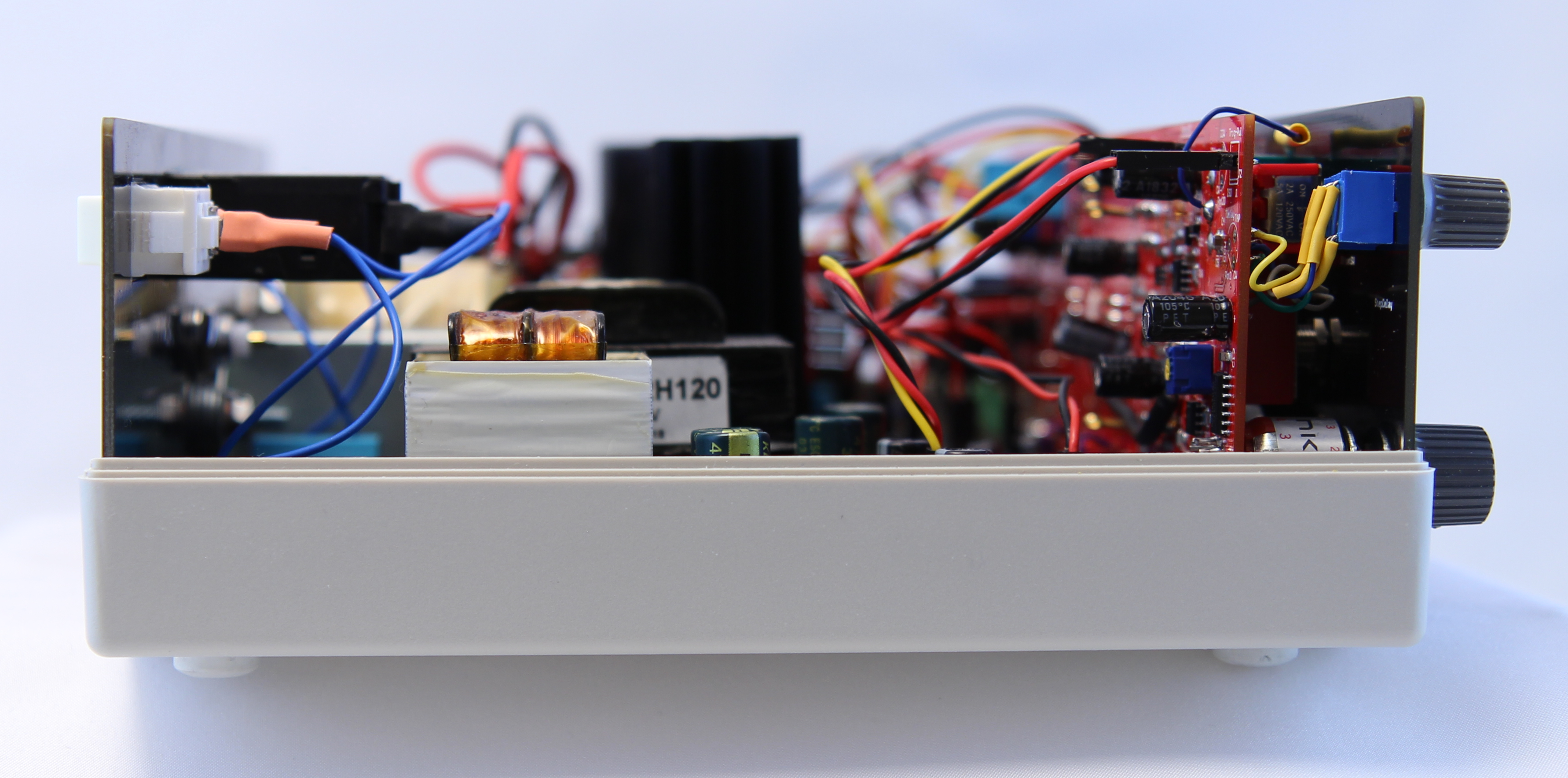
The Building Blocks
There are 4 Printed Circuit Boards (PCB's) that are used to build the instrument and will fit inside the enclosure. They are the Back panel, the Front panel, the Front board and the Main board.

These 4 boards and the circuits they contain will be explained below.
Note:
Some of it is already explained in the other posts (some of it has been removed and placed here) while using earlier revisions, but this Blog will only describe the final version that will be on the Github site.
Note:
The schematics I show here are converted PDF files to PNG in order to upload them to the Blog. The PDF files are exported from Altium Designer and have part numbers in them so they can be searched for in the PDF. These files and also the higher resolution and structured PDF files are available on the Github site, in addition to 2D and 3D images of the boards.
https://github.com/paulvee/VBA-Curve-Tracer
The Back panel
There's not much to it, just a black panel, reinforced with a ground plane on both sides with holes for the mains receptacle and filter, the main switch and the three BNC's that go to the scope. The two screws you see are used to mount the main transformer in a horizontal position.
The Front panel
The front of this panel, actually a black PCB with some components on the back, has the silkscreens for all the controls.
Note that this picture has the Y-amplifier silkscreen change, made since 17-Aug-2025 to better describe the functionality. There may still be some occurrences of the older version in the documentation and pictures. The name Y-Display Ratio for the toggle switch and the selections of 1V/A or 10V/A is more descriptive.

The back of the panel has the circuits to drive the four reverse mounted LED's. The Step Delay and Offset potmeters and the six 2mm DUT connectors are directly mounted on this board. The other controls are mounted on the Front board and protrude through this panel.
There are four special LED's that are used as indicators. They are mounted on the back of the Front panel and shine through little holes in the board to the front.
Top left is the Fault warning indicator, its function is explained in the Front board section. R10 and C4 are part of the R/C filter for the Fault circuit, also explained below. They are there to prevent a floating Gate of Q2 when the interconnect cable is not connected.
Top right is the High voltage indicator that is activated for DUT voltages of approx. 40V and higher.
The resulting voltage is clamped by D5 and fed to a transistor that turns on the LED.
Bottom left is the Power on LED and to the right is the Current Limit indicator. This LED gets turned on when the DUT current is at or above the maximum set current, protecting the DUT.
Both connectors have wires that go to the Main board, with the exception of the FaultOn signal, it goes to the Front board where the fault detection circuit is located and from there it also goes to the Main board where it is used to strangle the input to the DUT supply to remove the output.
At the very top of this blog, you can see the way I built my Curve Tracer, using knobs that came from Tektronix equipment.
Here is a picture of the CT that Mark built, using knobs that are listed in the BOM's.

The Front board
The circuits on the Front Board are first of all there to interface to the controls on or for the Front Panel. The Front Board and the Front Panel are connected together in a sandwich form and will be one unit.
The secondary objective is to put the circuits close to the switches and the DUT sockets to minimize cross-talk and avoid long connections to the Main board.
This side is facing the Main board:
The other side is facing the Front panel. The switches, potmeters and DUT sockets are mounted on this side.
The circuits on this board are:
The Current and Voltage Ranges
Top-left
is the circuit that deals with the Current ranges and current limiting
adjustment Pot100. The R100/R102 voltage divider creates a 1V reference
for this circuit. This voltages matches the 100mA through the current shunt resistor and therefore the DUT in the 200V range. This reference voltage can be adjusted by a rotary switch (S101)
using the parallel resistors R104..R109 into lower voltages, creating
the 1V, 0.5V, 0.2V, 0.1V, 0.05V and 0.02V reference settings for the x1, x.5, x.2,
x.1, x.05 and x.02 current multipliers for the main DUT 35V/2A, 70V/1A and 200V/100mA ranges. This will allow you to set very precise current limits for the DUT that can be further adjusted from 0..100% by Pot100 located on the Front panel.
When
the DC output mode is selected with S102, two things happen. First of
all the 7.5Vp-p triangle-waveform input to the DUT power supply is changed to a
7.5V DC level, and secondly, the x1 current range is changed into a 0.5x range
to limit the maximum current output to keep the thermals in check. In the DC mode, all current ranges and voltage selections stay the same, only the output changes from a triangle-based waveform to a DC level.
Bottom left is the potmeter (Pot102) that adjusts the main DUT supply voltages. It allows the user to set the DUT supply to 0..35V, 0..70V or 0..200V depending on the selected DUT supply ranges.
In the middle is S100, a special ON-ON-ON
type toggle switch with a mid-position that is wired to create the three
positions that are used to select the main DUT supply Voltage/Current ranges (35V/2A, 70V/1A and 200V/100mA) using circuits on
the Main board.
The D2A & Step Generator circuit
The input to this part of the circuit comes from the Triangle
generator located on the Main board. This signal is optically separated
from all the Step Generator circuits. The input is a synchronization pulse that will align
the steps with the triangle waveform transitions. Bottom left is the
Step cycle delay circuit built around a 555-timer. The potmeter (P2) has
a switch to activate this circuit, and will create a variable delay between
complete step cycles, that can have 1..7 steps. The two gates in series
with the sync signal enable/disable the pulses and reverses the polarity to feed them into a
CMOS 12-bit binary counter.
Four of the counter
outputs are fed to a set of resistors (a ladder circuit) that together form a digital to
analog (D2A) convertor to create the stepped waveform. This signal goes
to a buffer amplifier with a gain trimmer to prevent the D2A
section from any loading and also allows for the precise setting of the gain to calibrate for 1V per
step. The output of the stepped waveform also goes to an Opamp that
inverts the polarity and so we have positive going steps for N type devices
and negative going steps for P-type devices.
The
four 12-bit counter outputs also go to a CMOS BCD to decimal decoder
that resets the 12-bit counter after a number of steps, selected by a
rotary switch (S3), so we can create step cycles with 0..7 steps. The "zero" step position can be used for special measurements like leakage of a Bias in combination with the offset capability discussed next. This
reset signal is also used to restart the step cycle delay 555-timer after each finished
step cycle.
The Step Generator Amplifier
The input for this section comes from the previous circuit, the D2A
section. The D2A section provides positive for NPN or negative for PNP
stepped wave forms of zero to 7 steps and this signal goes to a buffered
output section. This input signal is summed by an Opamp
(U20B) together with the Volt output feed-back signal, coming from an Opamp
buffer (U22A).
The output of U20B goes to another Opamp (U20A) that does double duty by creating a positive or negative offset to the stepped wave form for BJT
devices. The activation of the offset is made by S22A, a triple-pole switch that selects the BJT or FET modes. The offset controls are on the front panel. The output goes to a
complimentary transistor buffer. The output from this amplifier goes
through a resistor, selected by a 16 position rotary switch (S21) that sets
the output current for BJT's or output voltage for FET's going to the DUT Base or Gate connectors.
In
the BJT mode, there is a feed-back loop from the output to Opamp U20A that also does double duty with the offset. The feed-back is
needed to keep the output to the DUT linear and compensates for the
junction voltage drop of the output transistors, the DUT junction drop or even drops in the case of Darlington configurations and
the likes.
The BJT offset is
typically used to create a Bias for the Base of the DUT so you can test the device
as if it was in your circuit. The offset range is +/- 7.5V. The maximum
offset range is influenced by the mA/Step setting, such that with lower
settings, the maximum offset also lowers in range. This wasn't designed
this way, it's how the circuit works. This also means that when you set a
Bias level for the Base, it changes with different Base currents, so
you need to readjust the offset for every Step setting.
The Voltage mode for FET's is created by
placing a 1K resistor from the output to ground through S22B, converting the output current to an output voltage. What goes to the DUT Base or Gate output connectors is selected by S22C. A similar feed-back
loop is needed in the voltage mode to create steps of the selected
voltage size. This will also create uniform range settings between the
current and voltage mode settings, making the front panel selection very
easy and straightforward.
The voltage mode also uses a different offset circuit and is enabled with S22A. Voltage
devices (FET's) typically need an offset to the Gate to get them in the
(VGSth) operating area and JFET's to put them into the pinch-off setting (Vp). The way Mark designed the FET offset circuit, the
VGS stays at the same level when you change the V/Step output.
When you change the
offset (VGS) to get a current to flow, devices can quickly overheat so it is prudent to set
the maximum current, use the step delay and use the offset carefully. This is why we selected +/-2V as the maximum offset by default to be able to select the right voltage level.
When
you often test low RDSON MOSFET's, you may benefit from a finer offset
adjustment for the VGS, and we have a 3- or 5-turn potmeter as an option for Pot20 that fits in the
tight mechanical space we have. Because these pots have a value of 10K, the value of R21 needs to be changed to 9.09K to create the 7.5V reference level again.
Depending on your testing needs, the offset range of +/-2V can also be changed to 1, 1.5, 2.5, 3, 4, 7.5V and 10V by changing three resistor values. The resistor values for these voltage ranges are in the BOM on the Github. In these cases, the 3- or 5-turn potmeters are even more desirable.
Because the input from U20A, U22A and the output of U23A can come in contact with the up to 200V DUT supply in case of a DUT breakdown, or user error connecting the DUT connectors, we have added several protection methods to protect the Opamps. First of all, the inputs are all clamped to the rails by diodes, and the inputs have rather large resistors in series to limit the current.
We have gone through great pains to protect all the Opamp inputs
from an accidental DUT supply injection, something that we found lacking in professional and very expensive equipment that have high DUT output voltages. We typically use high value
resistors in series with the inputs to limit the current and by using clamping diodes to the rails. We also use TVS diodes (D21 and D23) and a series resistor R37
to take care of the energy that will be dumped back into the supply
rails and also to prevent latch-ups. All the voltage regulators for the rails have diodes across them so the energy is dumped in the main electrolytes, while keeping the regulators safe.
The output of U23A is protected by two depletion-mode MOSFET's in a back-to-back configuration. This configuration acts normally like two low Ohm resistors at low
currents up until about 65mA, or when the voltage across the FET's is lower than +/- 1.5V. Here is some more
information about using depletion-mode MOSFET's
When
the voltage across these MOSFETs is positive and high, typically coming from the DUT
supply in the N polarity mode, Q22 is now a forward biased diode
in parallel with a resistor, and Q23 is a constant current sink of 65mA.
When
the voltage across the FETs is negative and high, typically in the P polarity mode, Q23 is now a diode/resistor and
Q22 is the 65mA current sink (or source, depending upon your perspective.)
In
both cases the current going to the Opamp is limited to 65mA, even though the
Fault circuit (described below) will remove the DUT output in a few Milli-seconds anyway.
During this short period however, the Opamp needs to be protected.
The
U23A Opamp output is further protected by two clamping diodes that dump the
excess voltages to the supply rails. To prevent latch-ups, a small
resistor (R41) is used in the negative rail.
So
these two back-2-back depletion-mode MOSFETs provide a low series resistance in normal operation, but limit
the current during an over-voltage fault condition to protect the Opamp if the DUT Gate connection gets a
high voltage across it. Without this current limit feature, the current flowing
into the protection diodes would be much higher and could trigger a latch-up
event or do other damage.
The Fault Detection circuit
To protect the Step Generator from DUT supply injection, we use the above circuit to switch the DUT supply off and prevent damages.
The above circuit is connected to the Gate or Base DUT connectors, and through series diodes for positive or negative voltages, go to two optical isolation circuits that are connected to the rails of the Step Generator circuits. The optical
isolation is needed to keep the Step Gen circuits floating from the Fault detection circuit and the rest
of the CT.
Depending on the P- or N-mode polarity, one of the opto-isolators will fire when
voltages of about +/-18V (just beyond the +/- 15 Volt supply rails) are detected on the output of the Step Gen amplifier Base or Gate DUT connectors. This will activate a set of BJT's that are configured as an SCR that trips. The resulting signal is going to an LED the Front panel that acts as a warning, and also goes to the Main board to remove the input to the DUT supply, in effect removing the output from the DUT connectors.
There is an R/C delay built in these circuits that will release the SCR after about 16mS. When the fault
is no longer there, normal operation continues otherwise the DUT output
remains clamped.
D121 is there to prevent false triggers when you switch the polarity between N and P devices. Remember that this switches the Step Gen Isolated Gnd to the positive or negative DUT supply side. (Look at S72B in the X-Ycircuit below) This switching can still cause a glitch that triggers the Fault circuit. Bud found an easy way to mostly prevent that from happening by adding a BAT54 diode.
The DUT X and Y Amplifiers
This
circuit has the X and Y amplifiers that feed the measured DUT Collector/Drain voltage and the Collector/Drain current to the DSO/CRT to create the I/V curves in the XY-mode of the DSO. The diagram also shows the connections to the DUT connectors.
The vertical Y amplifier measures
the DUT (Ic or Id) current across a shunt resistor (R80, 81, 86 and 90). These 4 resistors should in total be 1R0. The current through the DUT is converted to a voltage that will represent the current on the screen of the DSO. (Represented as V/A). The gain of the amplifier can be switched between x1 and x10 for low level currents, to amplify it and keep it out of the lower and more noisy V/Div. settings of the DSO.
There is an offset calibration circuit for this amplifier that can be used to adjust the output of the amplifier by +/- a few mV to align the signal to the DSO GND level.
The horizontal X amplifier has a gain adjustment such that the
Collector/Drain voltage can be calibrated against the DSO/CRT V/Div
settings, such that you have a 1:1 ratio between the DUT voltage and the voltage displayed on the DSO.
The
rest of this circuit deals with the rather complex switching of the DUT
polarity and also between the two DUT sockets that makes a comparison
between two devices easily possible. There are two DUT test sockets on the front panel that will allow quick insertions for different
pin configurations. There are also two sets of three 2 mm banana jacks
that can be used with flying leads and grabbers, or they can connect to a
separate PCB with SMD pads, or for other type sockets, like a ZIF
socket as we used during the testing phase.
The B/G signals have a small inductor in series to remove possible oscillations. The 2mm DUT connectors can be further dampened by adding optional capacitors between B/G to GND. These values should be below 100pF to avoid influencing the Stepped wave forms. If you use longer wires connected to the 2mm sockets, you should used shielded cables to keep the signals clean and avoid added inductance and capacity that can lead to oscillations. This is especially the case with higher voltages and currents.
The Main board
The circuits that are located on the Main board:
AC Power Supply
This circuit supplies the unregulated DC voltages for the DUT power supply.
We use two transformers to create the voltages for the DUT. The main transformer is either mounted on the bottom of the enclosure or horizontally screwed to the back panel, due to its weight. This transformer is actually a 56VAC/1A center-tapped version that we modify to split the secondary windings into two separate windings. This allows us to switch the windings in parallel to halve the voltage and double the current, and when we switch the windings in series we have double the voltage and half the current.
To create the 200 volt, we switch another transformer "on top" of the main transformer.
We do all this switching to create precise and stable voltage and current ranges for the DUT. One relay is used to switch the main transformer from serial to parallel, and another relays switches the high voltage on top. The switching is accomplished by a three position toggle switch on the Front panel that connects through J4. To avoid voltage spikes, we use one main capacitor that will absorb the range switching transitions. To quickly bleed-of high voltages, a relays is used to switch a set of power resistors in parallel when the user switches from the high voltage to one of the two lower voltages.
The voltage ranges we selected can be used with the maximum currents in these ranges. They are:
- 35V at 2A
- 70V at 1A
- 200V at 100mA
The transformers we selected have dual primary windings so they can be used in countries with either 110V and 230V main supplies. A switch is used to select either of these voltages for all the transformers.
DUT Power Supply
The DUT power supply is a regulated supply that can output a triangle-based waveform which is the default mode, but it can also output a DC voltage, mainly used for DUT leakage measurements.
Voltage Control
Top left is the input section for this supply. The input is either a triangle-based waveform of 7.5Vp-p, or a 7.5V DC level. With either of these input levels, the output for the supply can be calibrated to 200V with Pot101. When the user selects one of the two lower voltage ranges, the DUT supply input voltage is reduced by switching a resistance to GND by using two MOSFET's, Q108 and Q109. These MOSFET's get activated by the same switch that also selects the AC supply voltages. Pot100 and Pot102 can be used to calibrate the 35V and 70V output levels.
By using this technique, we make sure that the output of the DUT supply will immediately switch to a lower output voltage range when a lower range is selected, even though the higher unregulated input voltage of the supply will slowly decay from the higher level.
The output level of the supply can be adjusted from 100% down to about zero volts (minimum set by R118) by a potmeter in the feed-back loop that is located on the front panel. We have found that these potmeters can be at the maximum toleration of +/-10%, which will effect the calibration for the maximum output level of 200V. Another value for R112 can be used to compensate for the potmeter resistance toleration. The value should be selected such that with trimmer Pot101 at mid-level, the output voltage should be close to 200V, allowing a precise calibration with Pot101.
After the input reduction and voltage control, the input signal is clamped by two diodes to add some protection and is entering a trans-conductance amplifier
created with matched transistor pairs. The output of this amplifier is also protected with
another set of diodes and is used to drive the Gate of the main MOSFET,
Q104. The Drain is connected to the positive unregulated DC supply. The Source
connects through a little balance resistor via a choice of current sense
resistors to the main circuit ground. The 200V range DUT current sense resistor is R128, with a 10 Ohm value, and the DUT current sense resistors for the 70V and 35V ranges are switched in parallel by two MOSFET's, Q111 and Q112. These two MOSFET's are also driven by the main voltage range selector switch.
Keep in mind that the DUT supply as a whole regulates from GND downwards, like most higher voltage Lab Power Supplies do. Look at the other CT posts for more information. This effect can be noticed at TP100, the Positive DUT supply and TP104, the Negative DUT supply.
Current Control
The 10 Ohm value of R128 will create 1V across it when in the 200V at 100mA range. The values of R130 and R131 for the 35 and 70V range, and the resistor values of R132 and R133 for the 35V range will also have 1V across them with respectively 1A and 2A DUT currents. These voltages are measured with yet another trans-conductance amplifier which will compare the DUT current value with a reference value set by the Current ranges and the Current limiter potmeter, which enters the trans-conductance amplifier through the buffer Opamp U103A. When the current through the DUT is equal to or greater than the set current value by the user, the DUT supply will limit the voltage and thereby the current. An LED on the Front panel will indicate that situation.
To make sure the system can supply a net current of 100mA while in the 200V range, a compensation circuit is used to nullify any currents that the system itself consumes, in particular the approx. 12.5mA Current Source which will be explained below. The compensation circuit consists of R126, R135 and trimmer Pot103.
Dual MOSFET's to share the load
To lower the thermals that can develop inside the enclosure with the higher DUT voltages and currents, we share the regulation with two MOSFET's. U100A, which measures the voltage across the balance resistor R120 of the main MOSFET Q104, will drive the second MOSFET, Q105 to have the same current flowing through its balance resistor, Q117. This will ensure that both MOSFET's will conduct almost exactly the same current and so share the load. U100A has two output protection diodes that will prevent the output going beyond the rails and so protect it in case of a calamity.
R153 in the negative rail for U100 is there to prevent latch-ups when the output hugs the rail.
Step Gen Fault circuit
When lethal voltages find their way into the Step Generator, a circuit on the Front board detects that and sends a distress signal to Q106, coming in through J106. This over-voltage Fault detection signal will turn on the Q106 MOSFET and it will short the input to the DUT supply to GND, effectively removing the DUT output voltage. The detection circuit uses an SCR construction that has an R/C timeout of which half the circuit is on the Main board (R108 and C105), and the other half is on the Front panel (R10 and C4). This is done such that the Gate of the MOSFET never floats when an interconnect cable is pulled.
High Voltage Warning
This warning circuit is located at the very top of the schematic. When the instrument is in the DC mode, the DUT supply voltage is going
through a voltage divider made up of R2 and R6 in series and R8 to GND.
In the triangle mode, the signal is going through C28, that blocks the
DC voltage, and therefore has its own voltage divider made up with R3
and R7 in series with the same R8 to GND so the High voltage tripping point is about the same for both modes. The resulting low voltage warning signal goes to the Front panel where the high voltage warning LED driver is located.
DUT Supply Current Source
To improve the regulation of the DUT supply under all conditions, especially with no DUT current (no load) and minimum output voltage, a Current Source circuit is used. This circuit always draws about 12.5mA from the DUT supply, regardless of the output voltage that can be as high as 200V.
Triangle Generator
The DUT supply uses a triangle based waveform to activate the DUT and create the typical I/V curves for 3-pin semi-conductors, together with a step generator.
The Triangle Generator is the thumping heart of both the DUT supply
and the Step Generator. It creates the triangle wave form that is
the basis for the DUT supply, and it triggers the Step
Generator so the steps are aligned with the triangle transitions.
This 555-based circuit creates a free running oscillator that generates a square wave signal. The circuit is
also an integrator created by the feed-back capacitor of the output
Opamp to create a triangle waveform. The value of this capacitor and the trimmer in series with it determine
the triangle waveform shape and the frequency. The frequency can be
adjusted between about 140Hz to 650Hz. This will allow you to select the
optimum refresh rate based on the used DSO or CRT. The 555 acts as a
comparator. The R/C delay is set by C53 and the 200K trimmer Pot52.
Pot53 is there to
compensate for all the propagation delays in the Step Gen circuits,
mainly the opto-coupler, and is needed to precisely synchronize the triangle
transitions with the Step Gen step transitions measured at the DUT as they are viewed on
the display of the DSO.
The
output of the triangle wave form is about 7.5Vp-p and goes to the DUT Supply.
The circuit in the lower half with the two gates is used to create a trigger signal from the
square wave that creates the triangle transitions for the Step Generator. With these two Gates we can create a
single trigger pulse of either a positive going or a negative going transition, or
both, selected by two jumpers. This allows us to synchronize the
beginning of the Step sequence by either the top of the triangle, the
bottom of the triangle or have a step cycle strarting on either slope. The consequence has been explained in
the other Blogs and will be explained later in the Step Generator
circuit. At this moment, we are only using a jumper on P1-En. The other parts are optional. We decided to leave them in just in case there could be a use somewhere down the line for another maker. The output of the last gate goes through a pulse shape circuit to
create a better flank for the U53 opto-coupler output. The opto-coupler is needed because the complete Step gen circuit is floating/isolated from the rest of the circuits to allow polarity switching while keeping the I/V curves originating in the lower left corner of the DSO display.
On
the top of the schematic, there is a provision to create a positive going or negative going blanking
signal (Z-axis) selected by a jumper for CRT based scopes. This output is available through a
BNC on the back panel.
Triangle Power Supply Rails
We use a dual primary and dual seconday winding transformer. One separate secondary winding from the transformer is used for the Triangle
Generator, the DUT power supply and the XY amplifier. This supply
generates voltages of +10V and -5V. The +10V is used as a reference for
a few critical circuits, like the Current control so this supply can be calibrated with a trimmer.
The 7.5V section is used to create the DC level mode for the DUT supply. It needs a regulator because the current demands in the three main voltage ranges is different for every position.
Isolated Power Supply Rails for the Step Gen
The rails for the Step Gen circuits are +15V (called plusStep in the
schematics) and -15V (minStep). This
supply is floating (isolated) from all the other supplies and circuits and uses a
separate secondary winding from the transformer on the Triangle supply diagram to accomplish this. This isolation allows us to switch the Step Gen circuits to reference either one of the DUT supply rails, needed to keep the origin for both DUT N and P-polarities in the lower left hand side corner of the display.
XY Amplifier Power Supply Rail
This supply section is for the X-Y amplifier. The X-Y amplifier supplies the DUT voltage and DUT current to the DSO in the Y-X mode to display the results as I/V curves. It needs -5V (minusXY, the
same as minTri) and +24V (plusXY). We use a multiplier to create the 24V rail. Because the raw voltage after the
voltage multiplier is too high for a 78L24 regulator, we use a
transistor and a reference. The 24V is needed because we need a minimum
deflection of 20V from the X-amplifier going to the DSO to show the 200V Collector/Drain supply and
to also have enough head-room for the DUT current measurements made by the Y-amplifier.
That's about it folks...
It's a culmination of a project that took us about 3 years to complete.
On the dedicated Github site, you can find all details for this project, including the built instructions, calibration information, schematics, 2D and 3D pictures, BOM's and Gerber files. I highly recommend you order the PCB's through PCBway as they produced all the prototypes used in this project, and the quality is excellent.
For more information about this instrument and the way we ended-up with this result, have a look at the other posts on my Blog.
If you like what you see, please support me by buying me a coffee:
https://www.buymeacoffee.com/M9ouLVXBdw


38 comments:
Social, thank you for the detailed comments. For some reason, Blogger is blocking my replies to your messages so I'll do it this way.
You propose an interesting solution but at this moment we have no intention to modify the current CT design. It is important right now to get the details out first so others can build the instrument. If there is enough interest for your solution, we may have another look.
Hi Chris, all four of the boards have the standard thickness of 1.6mm and both panels will fit in the enclosure slots.
Hi Chris, these capacitors are hard to get, same with the main transformer. The version of the capacitor that's in the BOM is specified with a diameter of 35mm and a height of just about 64mm. You cannot exceed these two dimensions, the fit is too tight.
PCBWAY and JLPCB also sell parts, for reasonable prices. The total value should be 1 Ohm in total, you can use any value you want. Because it's the current shunt, use low values and keep an eye on the wattage. The DSO is probably 5% at best, so the values are not super critical.
Congratulations for the project, but why only Digi-Keys BOM? Why not Mouser too?
Mouser does not have all the parts Digikey has, besides, it's what we (mostly Mark) used in almost every order. It's not trivial to post a decent BOM and we have to start somewhere. BTW, the Digikey partsnumbers can be used with the Mouser part selection.
So, I gave it a go…
Frontpanel and Frontboard SMD parts soldered. All parts checked for values and/or shortages. All ok. Next step: Through Holes Parts and ‚sandwiching‘ them together. After that I’ll start with the Mainboard. I obtained all parts from Mouser, Digi-Key and some passive parts from Ali. Spent about $700 CAD on parts and $30 on the PCBs from JLCPCB. All soldered by hand, about two days (I have time, I am retired :). The 4R and 2R 2W resistors are unobtainable. So, for the 4R I stacked two 8R2 (5%, selected low value, ~8R) on top of each other. I arrived at perfect 1R (8x).
Update:
Frontpanel/Frontboard sandwich ready. Follow the instructions to the letter! It helps if you can make a few distance tools of 18mm length, e.g. from screw posts. Fit them between the PCBs and clamp the boards together. That way you ensure an even 18mm distance everywhere while fitting and soldering switches and pots. I used threadlocker loctite blue to secure the distance nuts on the switches because the tend to shift.
Two posts from me with pictures: https://www.diyaudio.com/community/threads/diy-curve-tracer-analog.379436/post-7207350
P.s. I have 4 sets of empty PCBs leftover.
For the 4.02R resistors I placed 8R resistor in parallel (8x; 4x2) ;)
I finished my device yesterday. It took my about 1 week net to solder and assemble everything. I soldered all SMD parts by hand carefully checking every individual component for shorts and/or bad connection. Thanks to the excellent instructions everything went smooth. The BOM and the calibration instructions need some tweaking. Just follow it through and adapt, some understanding in electronics is required :). I have a post full of pictures at diyAudio.com for those interested. https://www.diyaudio.com/community/threads/diy-curve-tracer-analog.379436/post-7207350
I plan to write a Python Frontend with the ability to save CT settings and transistor parameters as well as control a Rigol DS1000 oscilloscope and then storing transistor curves. Will see…
The project was fun to build and really rewarding since it was challenging for me.
Hi Tubekiddo,
Congratulations, this is not an easy project to finish!
If you could send me some pictures of your design, I will post it on the Blog.
Paul
Tubekiddo,
Do you still have extra PCB's? I would be interested.
Can get my email on QRZ.
Steve, WA0A
Hello sir. I would like to thank you for sharing this project. I have two questions.
First, you say that you do not release the Altium files to to preserve your ability to control the quality and protect yourselves from unauthorized manufacturing, but since the project is licensed under MIT, does that mean that anyone is able to alter the the files and make/sell this project?
Second, I was wondering if it is possible to substitute some of the potentiometers on the front board for carbon ones, since it would decrease the BOM cost considerably.
Best,
Christian M
Hi Christian,
1. We do not release the Altium files to prevent others from making a commercial product. All other information is provided.
2. Yes you can change the potentiometers. However, I would be very careful with the Voltage potmeter though because it must handle more than 200V.
Success with your build!
Paul
Calibartion and final assembly findings part 1/2:
During final testing of the main board I had no output from the DUT supply.
Found gate drive pulled to ground via Q114 in the overcurrent circuit.
With U101 input floating and not connected to the resistor network that makes up the current settings on the front board, this symptom persisted.
I made a mockup of the front panel current control network on a breadboard and connected it. This seems to have resolved the issue and brought the DUT supply output to life, although it continued to work properly once I disconnected my mockup.
I spent a long time trying to get the symptom to recur, which it did once or twice, but it became a circular process... and unfortunately along the way I managed to destroy U101 with a careless error.
I ended up with a new u101 and a new q114. All seems well now.
I can't say for certain that leaving U101 floating was the root cause here, but I did have the symptom recur a few times and each time as soon as I connected it to the current control mockup my DUT output came to life.
Perhaps this is worth mentioning in the instrux?
matt,
I'm on vacation for two weeks so it will take some time for me to work on your suggestions.
I fully agree with your comments about the two insertion connectors on the front panel, Mark insisted on them, I fought the same fight, and I ended up soldering the wires directly to the pads.
JLCPCB is not that happy, I received an email from them saying: "There is no keep out layer in your file, could we use the highlight outer frame of solder mask layer as board outline? (If there are cutouts in gerber file, please help to point out". Indeed there's no .GKO file in both the front and main boards while front and back panels do have it.
Anonymous, I have asked Mark to look into this and we'll have to wait and see see what he can do.
PCBWay has produced all our boards, including 10x of the Main and Front boards fully populated. The references to these orders are in the Blog. I strongly suggest you try PCBWay because they have proven to be able to produce all the boards.
Thank you. Sorry for the anonymous comment, it's just I don't want to register in yet another site. Posted it in your eevblog thread. I guess it would be enough to say to JLCPCB "yes, you can use outer frame of solder mask layer as board outline, no cutouts". I think that's what both JLCPCB and PCBWAY did with previous orders. Do you or your friend agree I could just say "go ahead as you say" to JLCPCB?
JLCPCB is reportedly cheaper and there were reports about orders made to them, but nobody so far got this answer from them. So no foreseeable problems... The gerbers uploaded perfectly and about an hour after that I got email saying the design had been reviewed, no problem. But about 12 hours after that, I got that second email about keep out layer. It looks I stumbled upon a quite wary production guy.
However I can see no reason why front and main board gerbers should lack this layer. By including them, any PCB house could do the work, no questions, no matter how expeditious/wary they are. So I'm just letting you know about it. But this is the first time I deal with this stuff and surely your friend knows better, so let's wait.
And many big thanks for your work on this, it's greatly appreciated.
I have passed the additional information to Mark as well. I have not heard back from him yet. He is the master of the EDA files, there is nothing I can do to help.
Anonymous, here is a link from a maker that used JLCPCB for the boards. Maybe this helps?
https://www.diyaudio.com/community/threads/diy-curve-tracer-analog.379436/page-2
Matt, I still need to research your "no output from the DUT supply" issue, but I need to be home in order to do that. It may take a while before I get to it though. My initial thought is that one of the Opamps slams into a rail, saturates and stays there (sticky effect), making it work.
I am glad to contribute any way that I can be useful! Not to worry, I am saving up my new comments and suggestions and, now that I am closing in on finishing this build and resolving issues I have been chasing down in the DUT supply, I will have some QUESTIONS! Ha. Enjoy your vacation, this stuff can wait
:)
Well, I can only assume that, if there was no keepout files in previous orders, surely they used the solder mask for that. I will give the "go ahead" next week, but any comments from your partner would be greatly appreciated.
I went back to look at the gerber files as they were distributed. At that time I was putting the board outline on every gerber plot. The Keepout layer was used for the cutouts in the inner parts of the board not the board outline or to keep copper out of certain areas of the board which is the intended use of this layer. This never has a use as a gerber file unless you are faking the keepout layer as a board outline layer. There is a keepout layer for the front panel PCB since it has the rectangular connectors on it for holding the DUTs. Some manufacturers use the keepout layer to indicate internal holes. This is not the intended use of the layer either. I have encountered several different uses of the varoius gerber layers. You have to decide with the board manufacturer what they want to use as the board outline correctly or incorrectly. At the time when I made 10 systems PCBWAY was allowing the board outline to be on all layers and not the keepout layer. I have had discussions more recently with PCBWAY. Among other things I got complaints about line thickness used for the lines depicting the board outline. So I decided to use the more industry standard of the .GM board outline gerber file. It uses 0 thickness lines for the board outline. Altium has this built into the design package so it was fairly easy to do. I no longer give a keepout layer unless there are internal "holes" on the PCB and that is how they want it indicated. In the description file I send with every PCB order I tell them exactly what the keepout layer is showing. I don't give it when there are no holes. The GM layer could also show the internal holes but I haven't needed to have any newer PCBs manufactured with them. Unfortunately I also get asked about the keepout layer when it is included on a board where the copper is supposed to be kept out. (This is the correct use of this layer). So no more keepout layer to the board manufacturer. The keepout layer is used by the PCB program to keep copper off a layer in a certain region. The gerber files never need to know this as the copper layer file will not have the copper in those regions already. So after all that verbal diarrhea can you tell me what they really want to indicate what the PCB outlines are. If they insist on using the incorrect keepout layer than I can send you some. If they will use the correct GM layer than I will send you some. The gerber layers JLPCB has, all have board outlines on every gerber layer. If you want to come up with a scheme that works for them and you let me know what it is and I will make that layer for you. I assume since the keepout layer was included on the front panel you don't need that one as long as JLPCB knows it isn't a board outline but the outline plus internal cutouts. You can continue on this blog or send the info directly via email if you prefer that. allie@wisc.edu.
Just to say that the actual boards manufactured by JLCPCB are fine. I've visually inspected them and checked their DRC advisory comments and I'm very happy with the results.
Well I gave the "go ahead" to JLCPCB yesterday. I think that, as Alastair says, the boards will be fine. Anyway, happy to know what to say to JLCPCB -or any other PCB house- should this question arise again. I will link your answer on EEVBlog thread. I think it's more than enough. I greatly appreciate your offer, but I think it isn't necessary anymore. Sorry to bother you. And big thanks for your work.
Hey no bother. The work was fun or else I probably wouldn't do it. Way back when I used to provide the board outline on the *.GM2 gerber plot.
I've picked up a couple of BoM errors for the Main Board:
1) C28 is shown on the bottom, but is on the top of the PCB
2) More importantly, the DigiKey part number for R132 and R133 is for 1R0 resistors, not 2R0. This affects the current limit for the 35V range and could cause problems. Potentially you could just fit a single 1R0 resistor for R132 and leave R133 not fitted, which I think will dissipate 0.37W on sweep at full current, but my calculations could be wrong!
Hi Alistair, thank you for the remarks. The mfg p/n for the resistors is correct, the Digikey p/n is not, I'll fix that. I'm not at home so cannot verify the position of C28. I'll fix it when needed and update the BOM with both corrections.
Great project! I just downloaded it from guthub. Unfortunately the PCB-outline is missing in the Gerbers folders for Main_board and Front_Board. ;-(
The so called missing outline has been debated with several suppliers. They can produce the board without any issues however.
Thank you to the VBA gang for this great project. Finally finished mine and got it all working. I had numerous problems to over come but they were all my fault. Also burned up one set of MOSFETs when I accidently shorted ISO GND to GND. All the documentation was great. Thanks again. Bruce
Hi Bruce, congratulations and thank you for posting, well appreciated!
Also thank you for the Java contribution!
I'm in the process of completing the CT, but I got stuck on point number 61: "We also need to connect the 100K Volt potmeter between one of the J102 pins called Vset
(CCW) and DUTSupplyM/TransM (Tap+CW) so we have an output, and we can set the level. Set
the potmeter to about mid-range. " How should the potentiometer be connected to get a negative going triangle waveform?
The triangle waveform is going negative to Earth GND when you measure it in this step. It does not matter how you connect the potmeter, as long as the turning direction is what you expect. (turning clockwise for a larger amplitude)
What's a price for the parts required?
Unfortunately there are some expensive parts involved -- specific rotary switches and pots, trafos, the case, etc... and it adds up. When I built mine over a year ago I think the grand total came to about $6-700 USD
And you are unlikely to have many of the parts in stock at home. There is some scope to trim costs a bit, but I doubt the total will be less than £500 GBP / $600 USD
Post a Comment